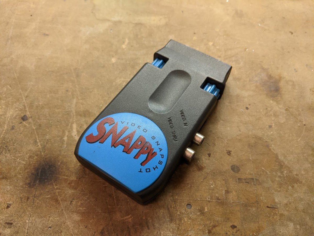
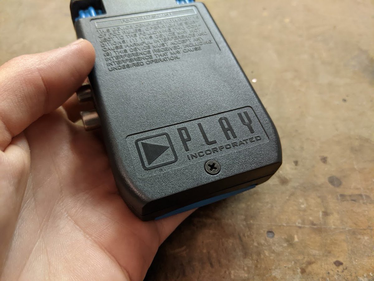
here's a fun piece of (very) 1990s hardware: the Snappy Video Snapshop, from a company called Play, Inc. it is a video digitizer, so video goes in one end... 
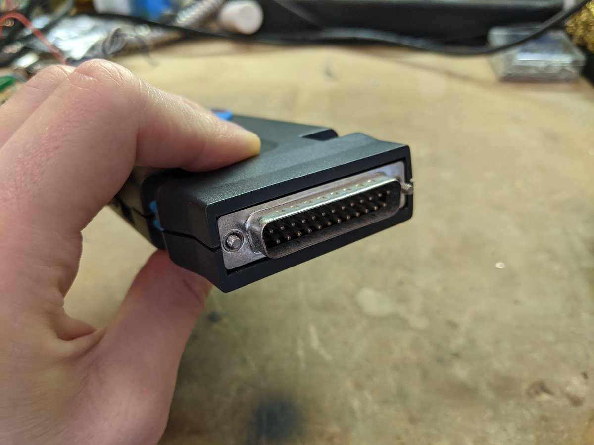
...and the other end plugs into your computer's *printer* port! no USB back then, so this was how many peripherals connected to your computer, including CD-ROM drives, tape drives, even network adapters.
let's try it out! i found the software, thanks to saao.ac.za/~wpk/snappy/so…
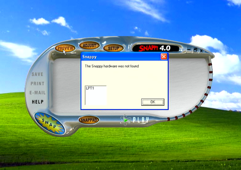
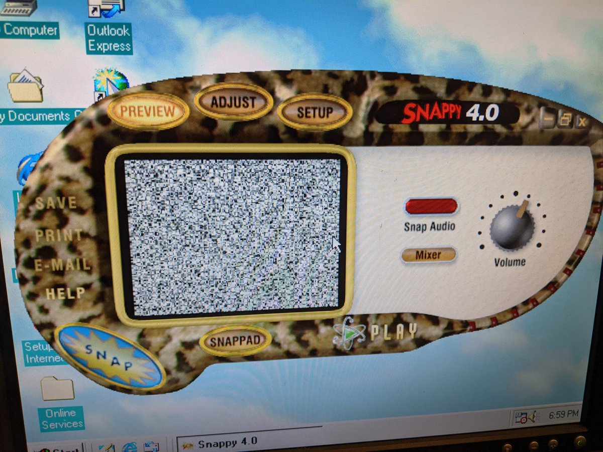
hmm, no dice. what's going on?

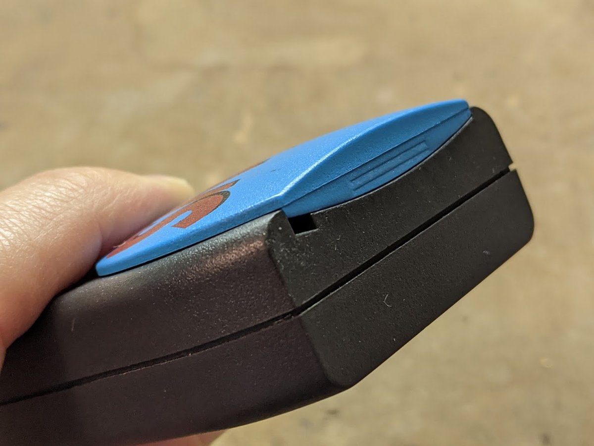
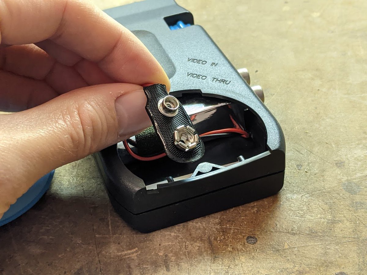
turns out, i forgot to put in a battery! you lift up the blue panel and it reveals a 9V battery compartment. the printer port did not provide power, so some peripherals used an AC adapter while others used a battery.
no luck, unfortunately. i tried a bunch of different things (EPP vs bidirection LPT1 mode in the BIOS setup screen, etc) and nothing works. i think this Snappy is broken. 🤔
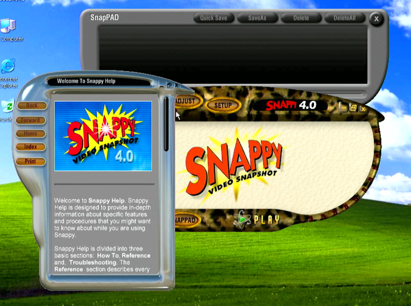
gotta love the '90s themes here. "Lounge" 😂
Also the non-rectangular window was super popular back then and surprisingly tricky to implement using Windows API.
Also the non-rectangular window was super popular back then and surprisingly tricky to implement using Windows API.

omg every window in the program is like this 😂
anyway, let's take it apart! there are only three screws, accessible on the back of the device.
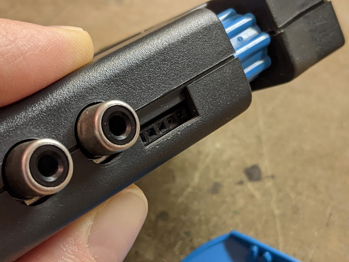
oh almost forgot to mention. next to the video in/thru ports there is a mystery 5-pin header.
inside the box is...another box! this is cardboard covered with foil and helps reduce radiated emissions (EMI).
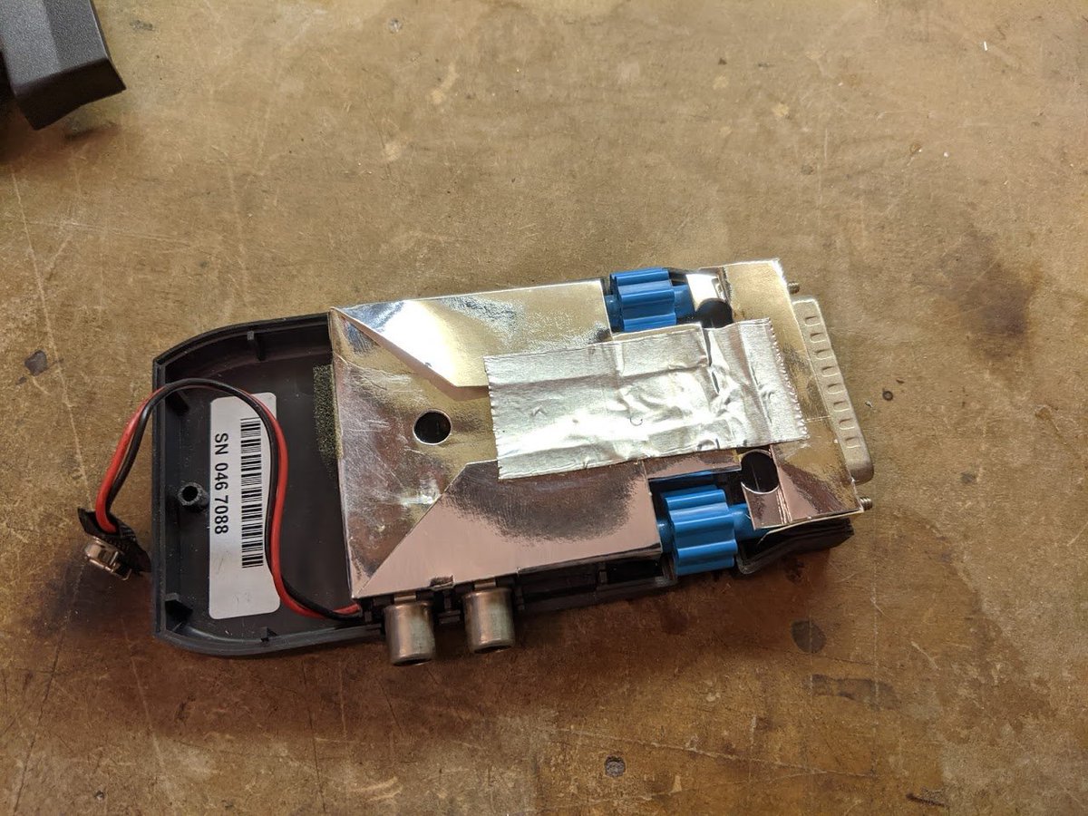
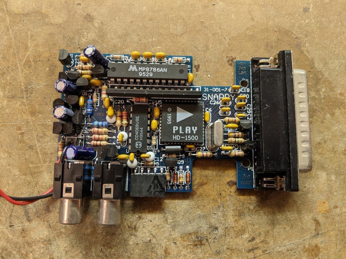
the christmas present is unwrapped, and there's a circuit board inside!
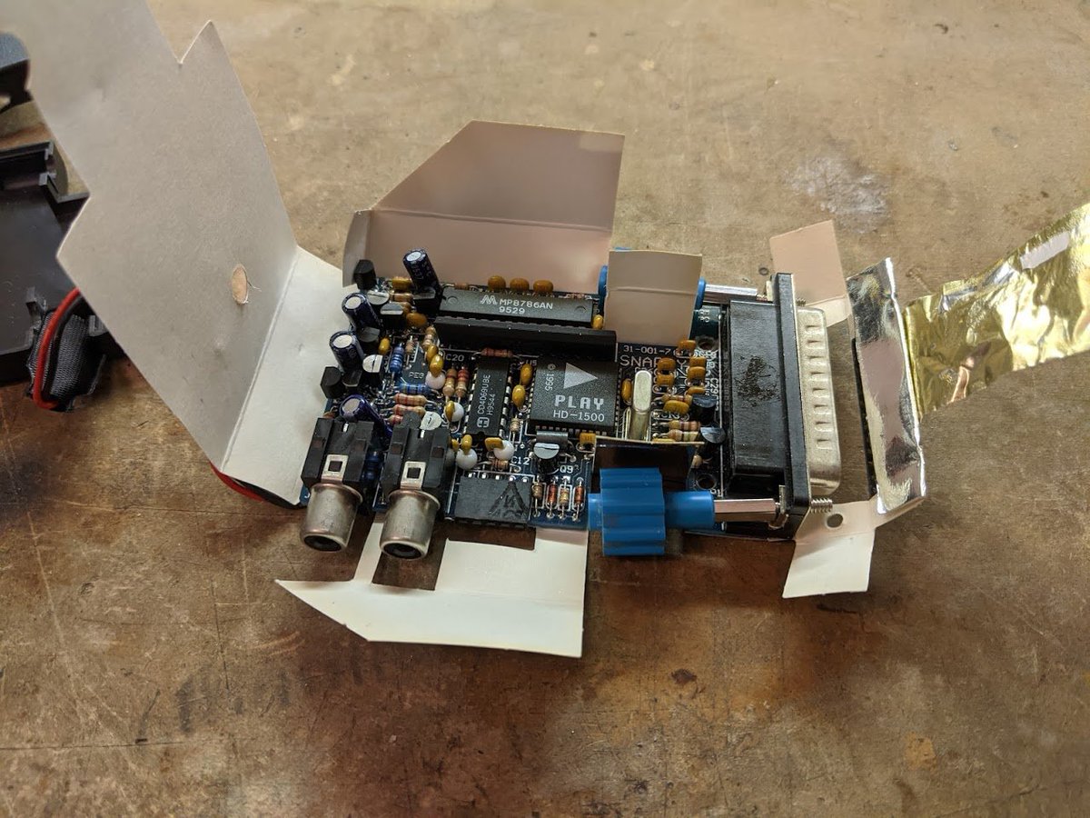
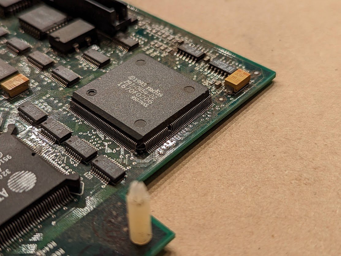
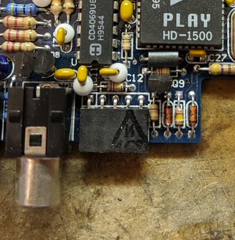
here it is up close. there is quite a bit crammed into a small space. interesting how it only has one surface mount IC on the whole board.
here's the back of the board. made in USA, interesting. and copyright PIT (maybe someone's initials?)
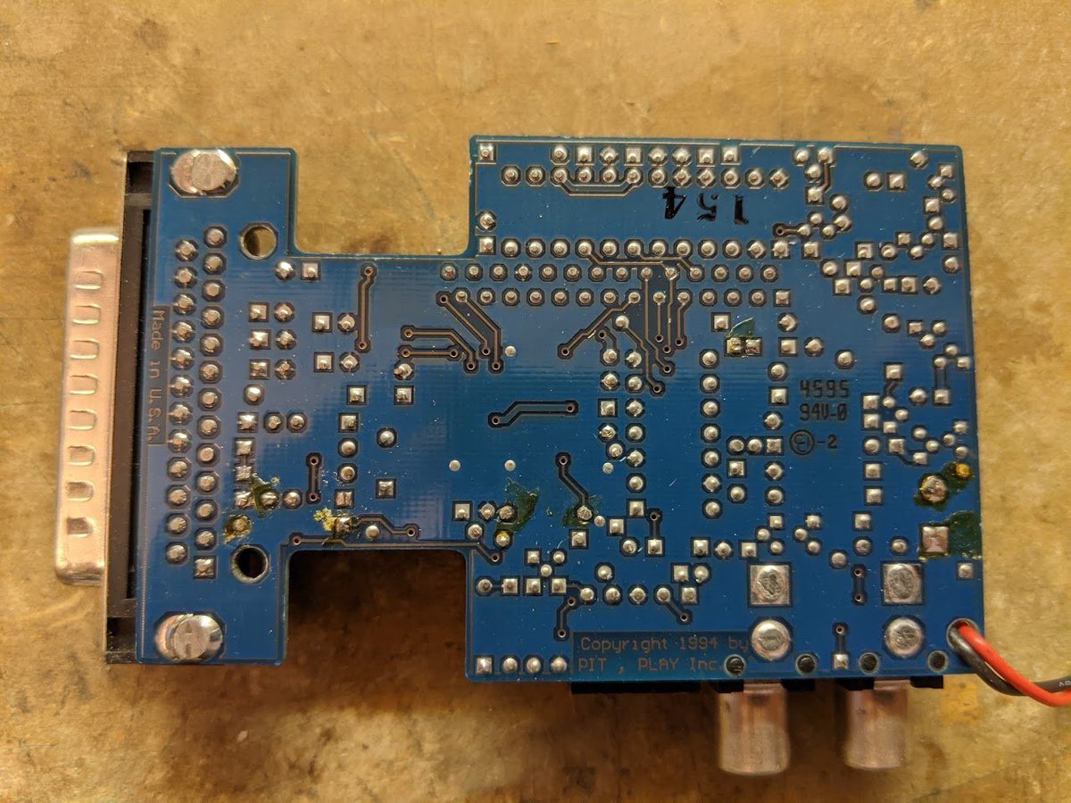
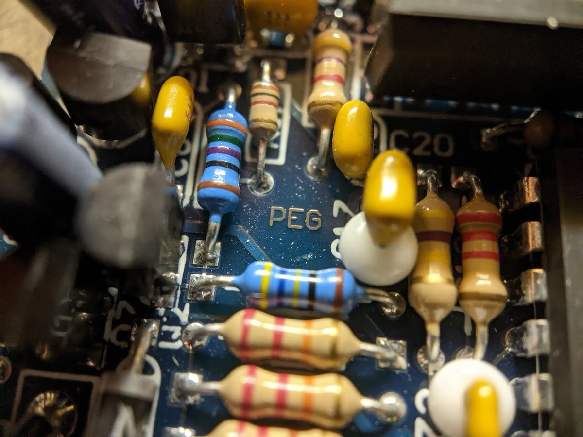
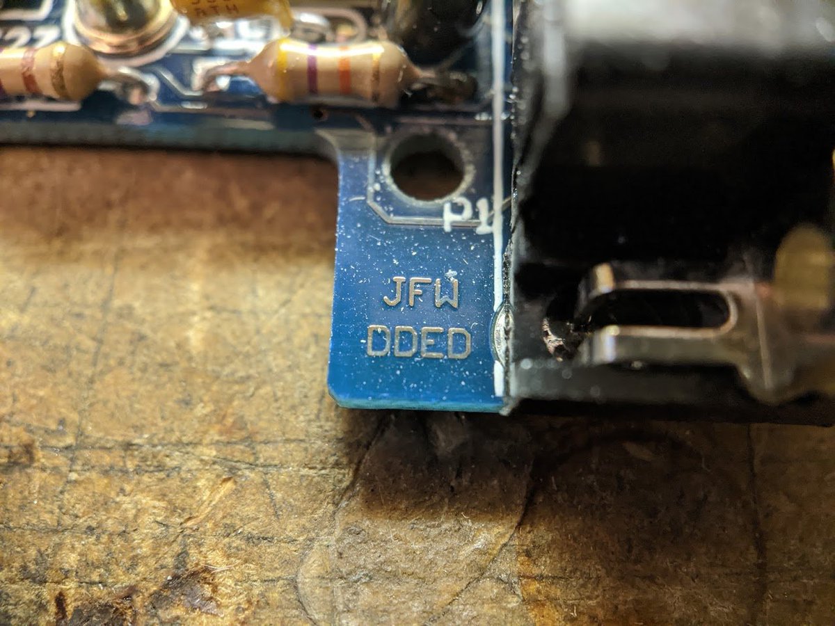
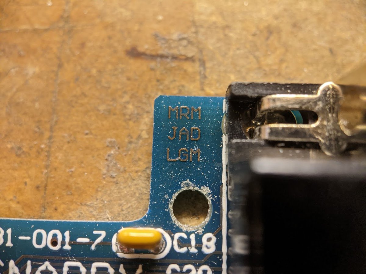
there are more initials on the top of the board. PEG, JFW, DDED, MRM, JAD, and LGM. if you know who any of these folks are, let me know!
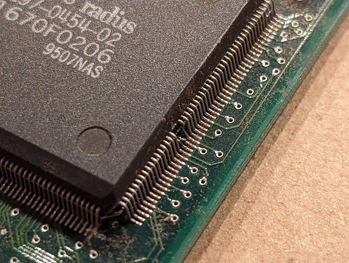
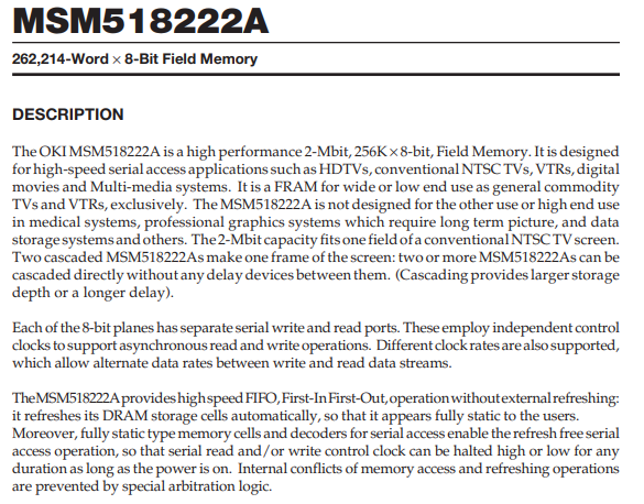
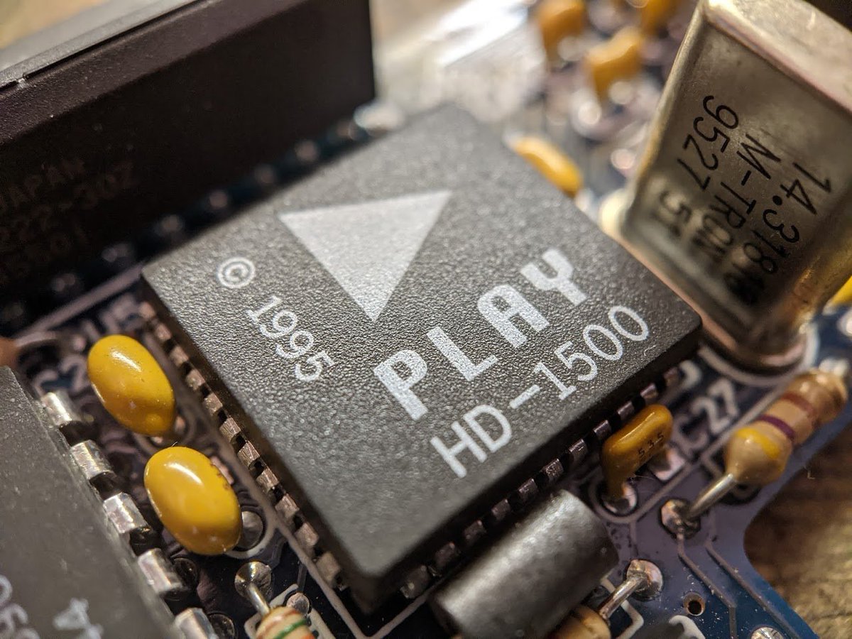
but back to the device. in the center is the only surface mount chip, this 44-PLCC marked "PLAY HD-1500"

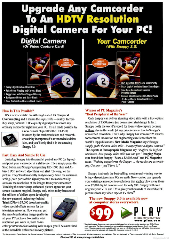
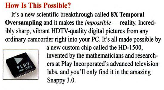
PC Magazine, june 9, 1998 has an advertisement for the Snappy which includes a picture of the chip.
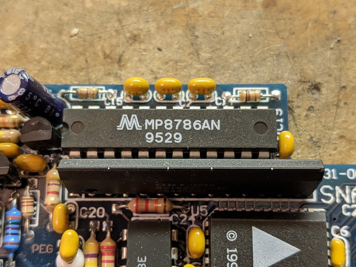
other devices include this 8-bit ADC. it is quite fast at 30MSPS (million samples per second). this turns the analog NTSC signal into a digital data stream.
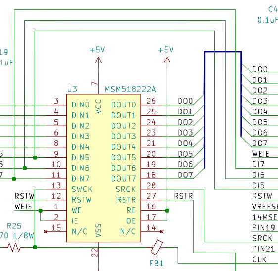
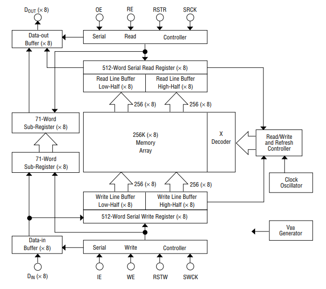
this other chip is a very special memory IC, the M518222 from OKI.
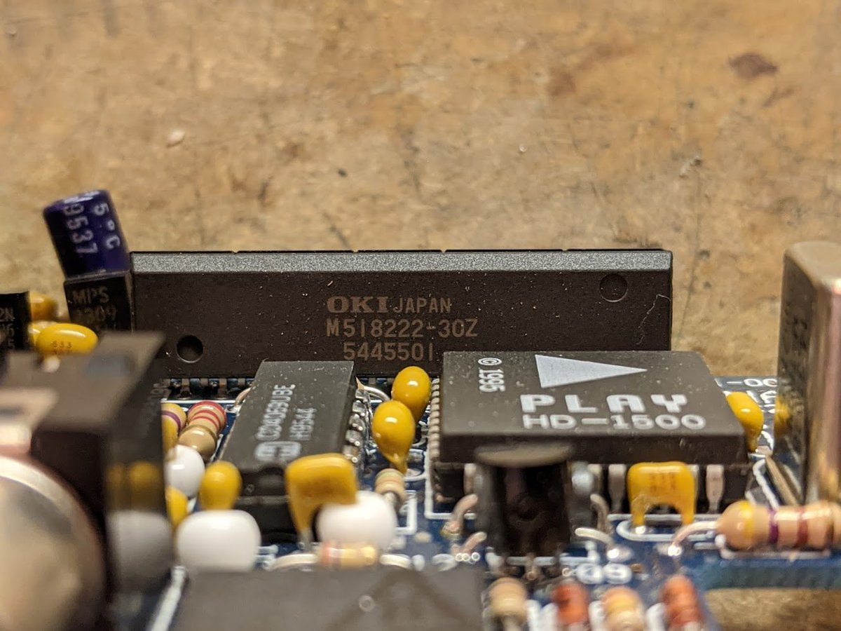
it is a special-purpose DRAM chip configured as a dual port RAM, and it is designed to store an entire NTSC field, which is every other line of a frame (due to the interlace). these chips were frequently used in scan converters.
the 8-bit data from the ADC goes to the input port, all you have to do is generate the sync signal and a pixel clock. then once you have a field stored, you can read it back at a much slower rate through the output port.

so it goes something like this: NTSC from the ADC to the RAM (1), RAM to the HD-1500 (2), and HD-1500 to the parallel port (3).
i'm very curious to find out what the HD-1500 is. is it a microcontroller? CPLD? DSP? something else, like a gate array?
the usual way is to check the power and ground pins first.
GND: 1, 16, 23, 28. VCC: 8, 12, 17, 33. the output data from the RAM connects to pins 42, 43, 44, 2, 3, 4, 5, and 6 (in order from D0:D7). so that's a good candidate for a GPIO port.
GND: 1, 16, 23, 28. VCC: 8, 12, 17, 33. the output data from the RAM connects to pins 42, 43, 44, 2, 3, 4, 5, and 6 (in order from D0:D7). so that's a good candidate for a GPIO port.
it's not an 8051-like device (most of which have very similar pinouts)
nor is it a 68HC705 or similar.
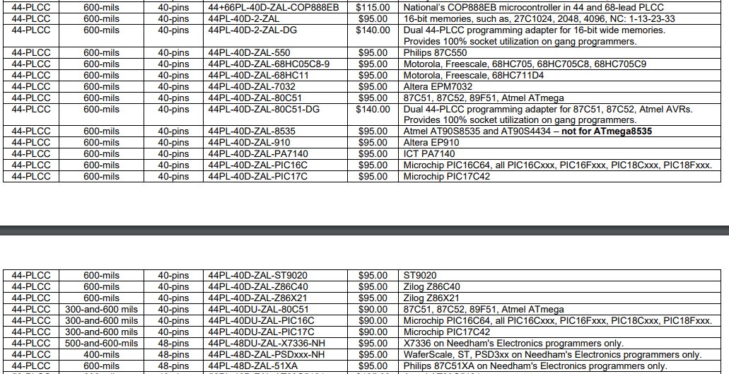
i also looked at CPLDs. pretty much everything i could find in 44-pin PLCC did not match up at all. it's useful to look at the socket adapters or device support lists from the various device programmer manufacturers.
there's very little information on the web about Play, Inc. the company doesn't even have a Wikipedia page, but is mentioned in a few spots including the article on Paul Montgomery who left Newtek (of Video Toaster fame) to found Play: en.wikipedia.org/wiki/Paul_Mont…
tried it on a win98 machine and it still doesn't work. the oscillator doesn't even run so i think it's probably broken. maybe i should just reverse engineer it. 😂
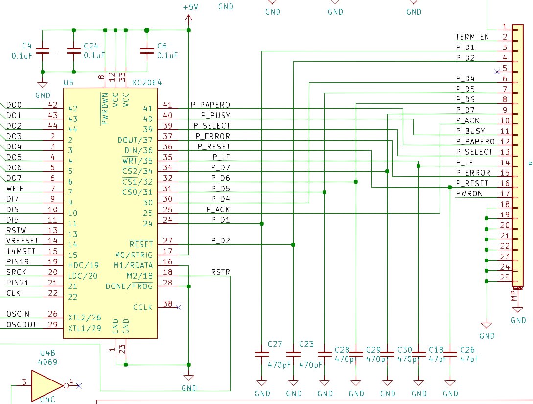
thanks to @kc8apf and @PhilipFreidin the mystery chip is an XC2064 FPGA!
wiring:
M2 (floating, seems like)
CCLK nc
DIN 16 [pport reset out]
DOUT 15 [pport error in]
WRT 14 [pport line feed out]
CS2 9 [pport db7]
CS1 8 [pport db6]
CS0 7 [pport db5]
RESET 4 [pport db2]
wiring:
M2 (floating, seems like)
CCLK nc
DIN 16 [pport reset out]
DOUT 15 [pport error in]
WRT 14 [pport line feed out]
CS2 9 [pport db7]
CS1 8 [pport db6]
CS0 7 [pport db5]
RESET 4 [pport db2]
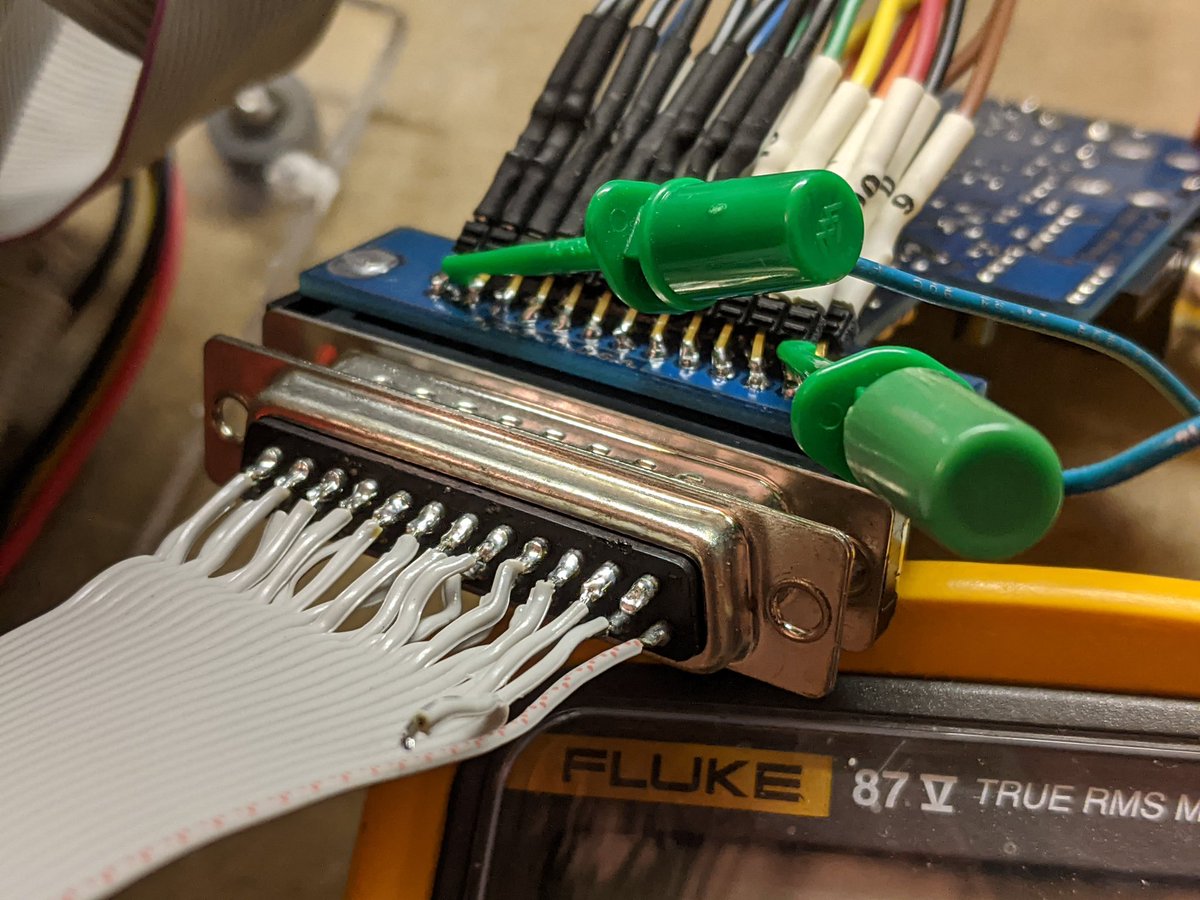
the important bit is that this FPGA can be programmed from the host software through the parallel port! that means i can spy on it with a logic analyzer.
and the mystery connector on the side? i think it is for manufacturing test. pinout is:
1. video
2. +9V power in
3. gnd
4. FPGA pin 19 (HDC) which goes low after programming
5. FPGA pin 21. purpose unknown.
1. video
2. +9V power in
3. gnd
4. FPGA pin 19 (HDC) which goes low after programming
5. FPGA pin 21. purpose unknown.
so it could still be possible that Play used a ROMed XC2064 for volume production and what i am seeing is a vestigial development convenience. but why not hook up a logic analyzer anyway? it's more fun that way!
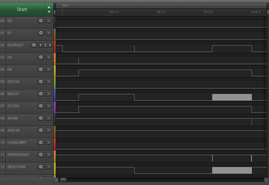
so winXP showed no activity at all, but on win98 i get this, and nothing is detected by the software. looks like it is trying to do something, but i am not sure what.
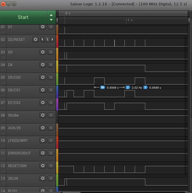
looks like it's never driving line feed aka WRT# low, which would start the programming process on the FPGA. it does everything else. 🤔
let's pull WRT low manually. grr. I've disconnected it from the PC side so I don't destroy the output driver.
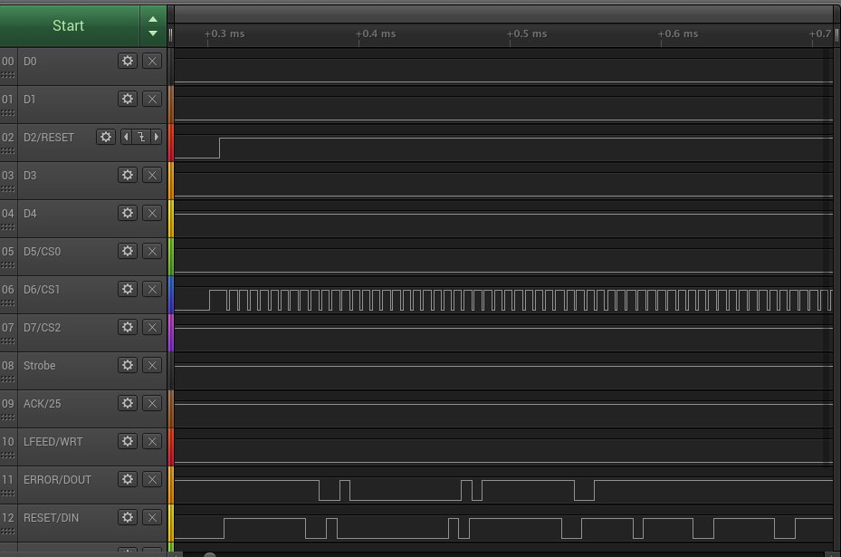
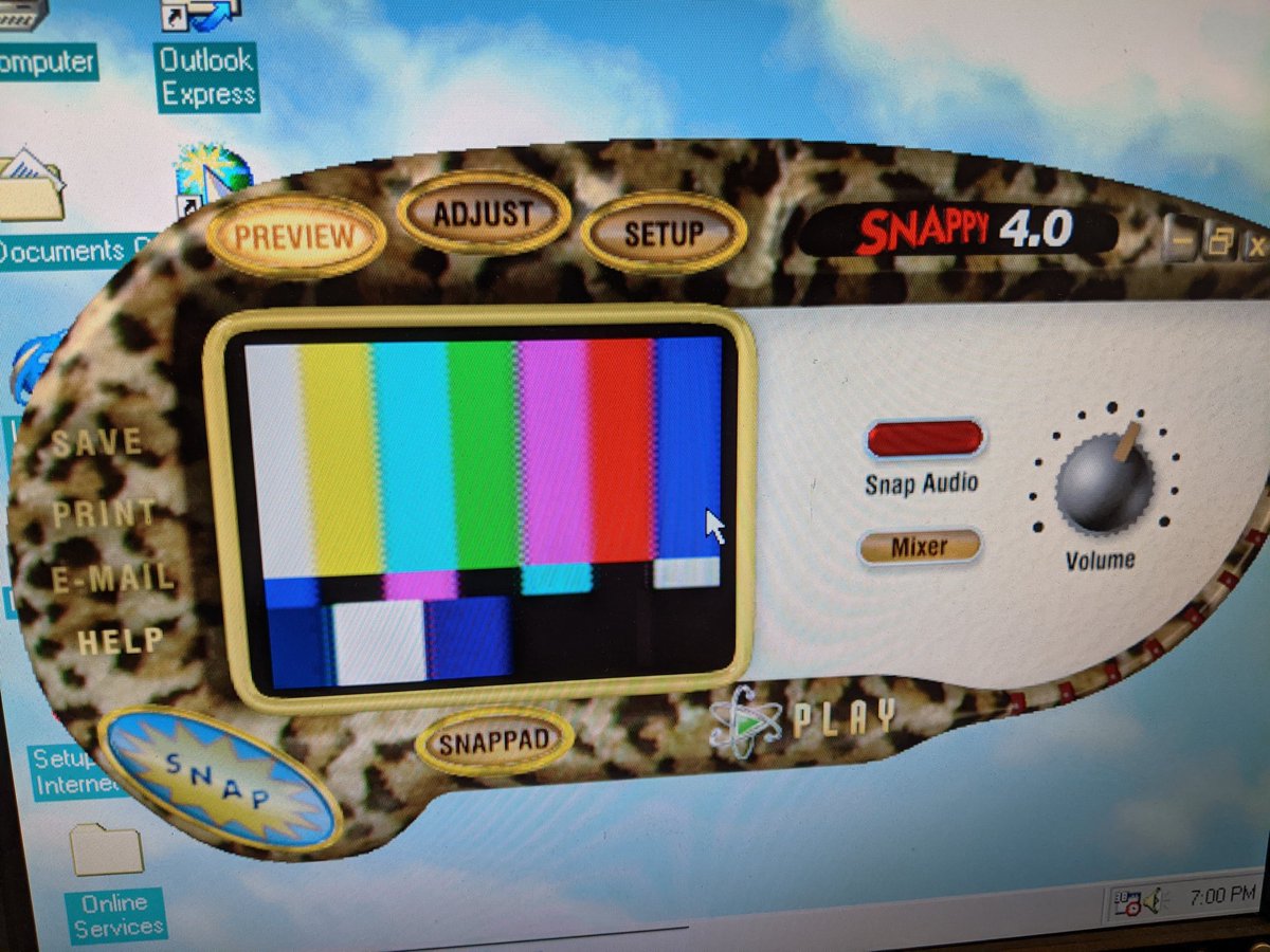
no error this time!
and it transferred data! the device is in peripheral mode.
bitstream!
static
color bars!
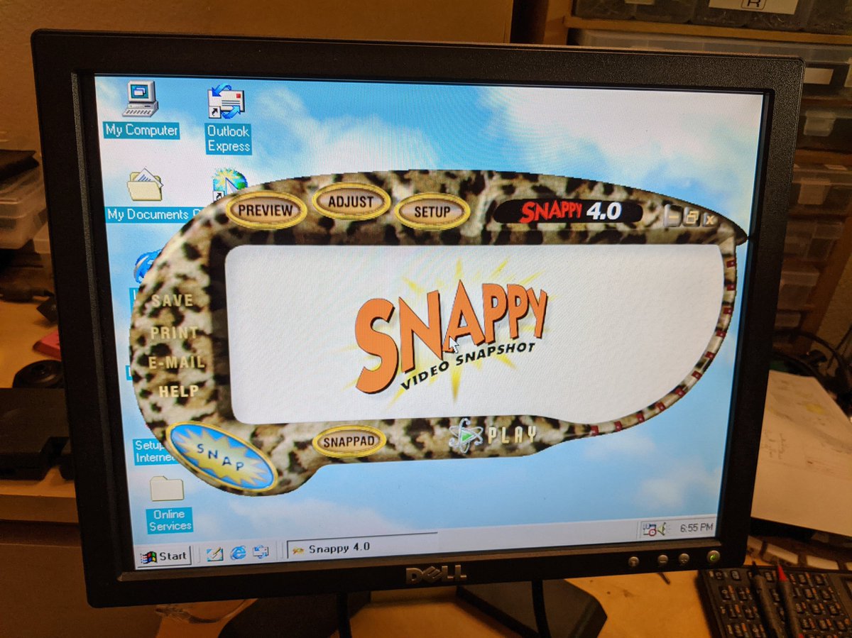
the Snappy Video Snapshot from 1995 (check out that UI!) has a live video preview mode! it's a bit slow and seems to be optimized for analog video from the 1980s for some reason 🤔
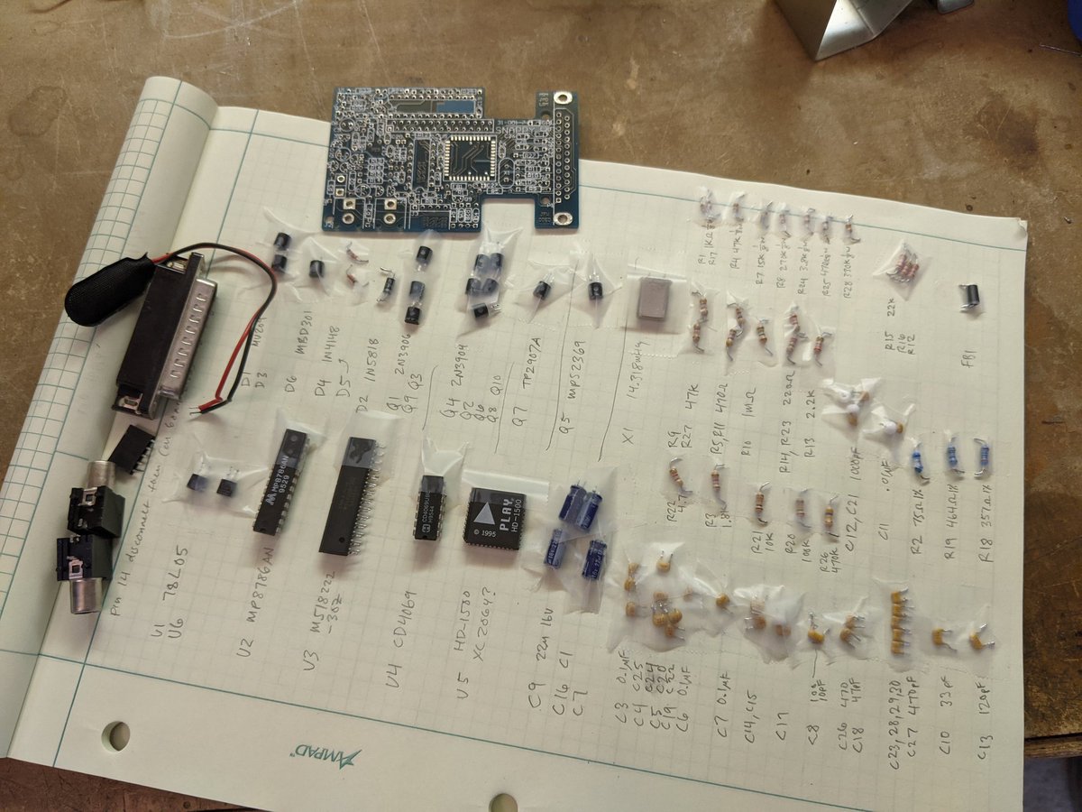
i'll reverse engineer it now. i've removed all the parts and turned it into an electronics kit 😂
here's the full schematic! it's a really fascinating design that i'll go through in more detail.
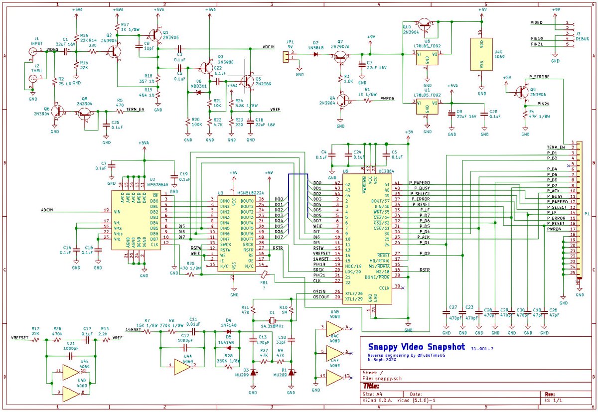
here i've called out the individual sections, and i'll go through them one at a time to explain how they work.
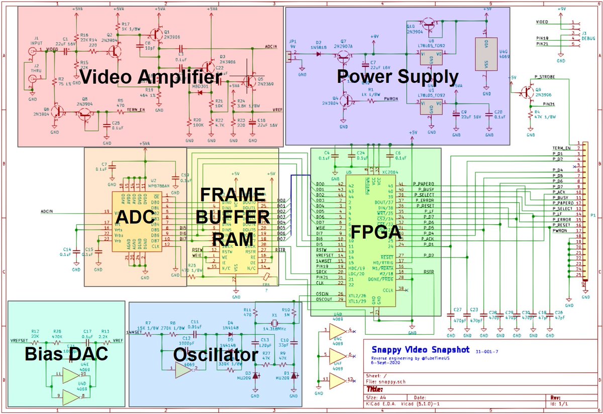
first up we have the FPGA. it has custom markings on it but it is really just a standard Xilinx part, most likely an XC2064. it is unprogrammed on power up, and the bitstream gets loaded by the PC software over the parallel port when you start it up!
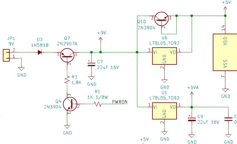
i guess i should mention power. it has a power save mode: the PC software flips on a bit (the printer select line) and this turns on Q4 and Q7, which provides 9V to the two 5V regulators, one for analog and the other for digital. D2 is reverse battery protection.
the video amp is interesting too. (primary signal path in red). Q1 and Q2 are common emitter amps, C8 is a miller cap to slow things down. Q3 and Q5 detect the sync pulse and restore the DC level, which is adjustable by VREF. Q6/Q8 can turn on 75 ohm termination.
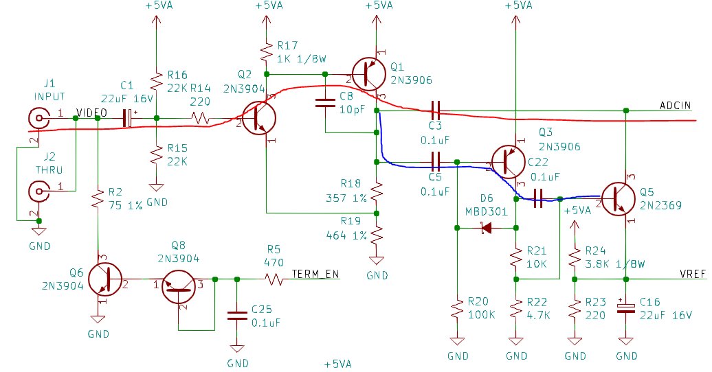
TERM_EN goes to the parallel port's D0 data line so the host software can control the termination. when you connect something to the Snappy's video thru port, you have turn off termination since the other device will provide that.
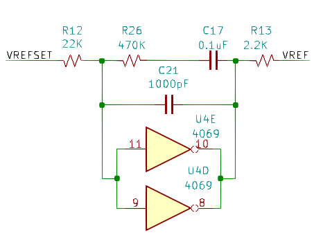
VREF comes from this bias DAC, which is VERY unusual. VREFSET is a PWM or PFM signal from the FPGA, and U4 is an unbuffered hex inverter configured as an inverting op-amp!!!
how does that work? think of the voltage transfer curve plotting Vout vs. Vin. it is equivalent to an op amp with the + terminal set to about 2.5V. (the 2nd device just increases the drive strength)
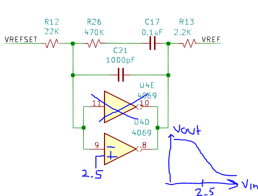
so why would you ever use an inverter as an op amp? well, it's super cheap and you get six of them in a single IC package. it's not a common trick anymore but back in the day designers used it all the time.
going back to the circuit, this integrates the digital signal from the FPGA, providing an analog control voltage that allows the NTSC video to be shifted higher and lower in voltage.

next up, we have the MP8786 high speed (30 million samples per second) ADC. this converts the analog waveform (between 0.6V and 2.6V) to a digital signal from 0-255. the clock comes from the FPGA, and i suspect it is 14.318MHz (4x the 3.579MHz NTSC colorburst)
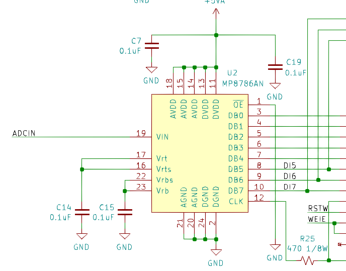
here's the dual port RAM which digitizes a video field and lets the FPGA read it at a much slower rate, feeding it out through the parallel port. something interesting: bits 5, 6, and 7 from the ADC split and run into the FPGA directly. why?
i haven't measured the actual board, but i believe these 3 bits are used by the FPGA to detect the sync pulse and the colorburst. it needs the colorburst so it can synchronize the 14.318MHz oscillator so that the sample clock is locked. this helps recover accurate color hue info.
here's the 14.318MHz oscillator. the FPGA has an internal crystal oscillator circuit, but there's some trickery here with D1/D3. these are varactor diodes--special diodes whose capacitance changes depending on the applied DC bias voltage.
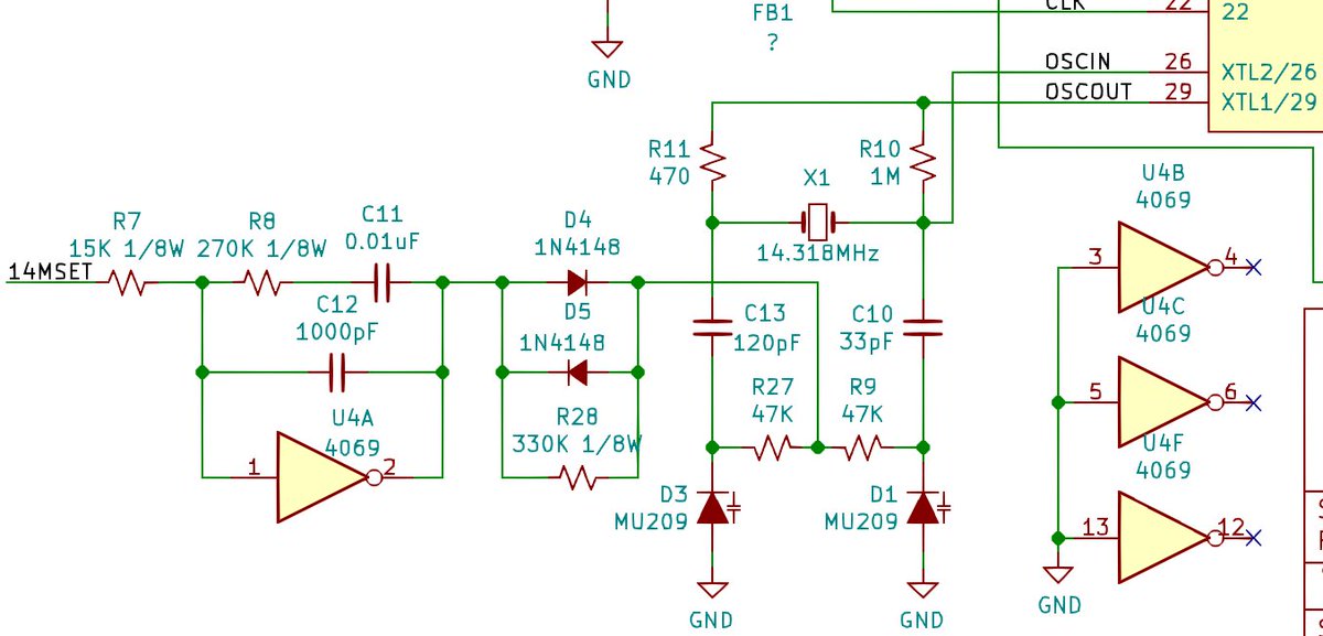
C10 and C13 prevent the DC bias from entering the clock circuit. by changing the voltage driving R27/R9, you can trim the 14.318MHz frequency up and down!

the FPGA does this using another CMOS inverter-as-an-op-amp, U4. PWM/PFM in, DC out. D4/D5 provide course trim: if the op amp slews dramatically, one of the 2 diodes turns on and pulls hard on the trim voltage. otherwise it goes through R28 which provides fine trim control.

so the conversion process goes as follows: FPGA adjusts video bias until it lines up the three MSBs (5, 6, 7) with the sync pulse and colorburst signal (basically using the ADC as a set of free comparators). then it adjusts the 14.318MHz oscillator to line up with the colorburst.
since it has locked to the NTSC sync pulses, it can send the "start acquisition" signal to the dual port RAM at exactly the right time. it continues until a whole field is captured. then, over the serial port (most likely in a serial data stream) it clocks the data out to the PC
some things i don't understand yet, like if the FPGA itself decodes the NTSC color subcarrier or if that's done in the PC software. it may very well be done in the FPGA, which explains how it can drop the resolution and increase the frame rate.
finding out all the remaining details would require reverse engineering the PC software and probably the FPGA bitstream, which is really more work than i am willing to put in.
the Snappy is a wonderful little jewel of a design, making maximum use of a small number of low-cost components in very clever ways. the engineers at Snap worked very hard on this, and it really paid off for them.
i reassembled it today! this time i made a video. let me know what you think.
• • •
Missing some Tweet in this thread? You can try to
force a refresh