a short but highly technical history of DRAM - dynamic random access memory! 🧵 
but first: dynamic?
static - a logic circuit that operates down to 0Hz clock.
dynamic - a logic circuit with a minimum clock frequency.
static - a logic circuit that operates down to 0Hz clock.
dynamic - a logic circuit with a minimum clock frequency.
static RAM is made of two cross-connected inverters along with two pass gate transistors that connect and disconnect the memory cell to the bit lines. you need 6 transistors to make a cell that can store one bit of information.
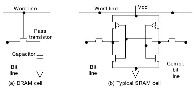
dynamic RAM cheats a little and uses a capacitor to store the bit instead. over time, this charge drains away so you have to periodically read the current state and then write it back again. it's like refilling a leaky bucket.

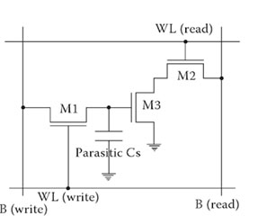
here's a more detailed diagram of the basic DRAM cell (3 transistor). the bit is stored in the gate capacitance of transistor M3 (shown as "parasitic C"). M1 is closed to write to the cell and M2 is closed to read from the cell.
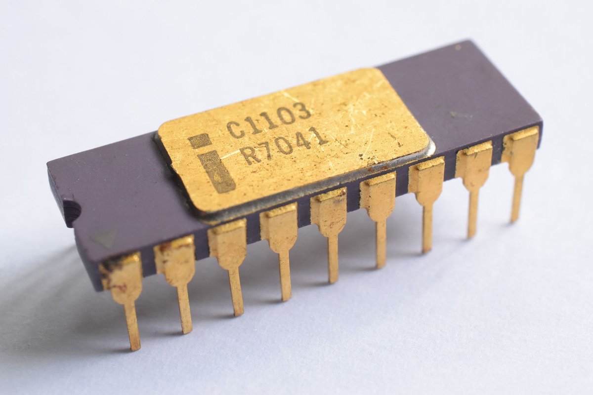
now back to the history: this is the first practical DRAM chip, the Intel 1103, which they introduced in 1970. it was expensive at 1 cent per bit (1024 bits total). that's about $7 now. you'd need two of these chips to store the text in this tweet!

here's the pinout. address lines, chip enable, data out (inverted?), data in, read/write, precharge (similar to a clock line), and then three (!) power rails: VSS=+16V!, VDD=GND (PMOS is weird) and VBB=+19.5V(!!!)
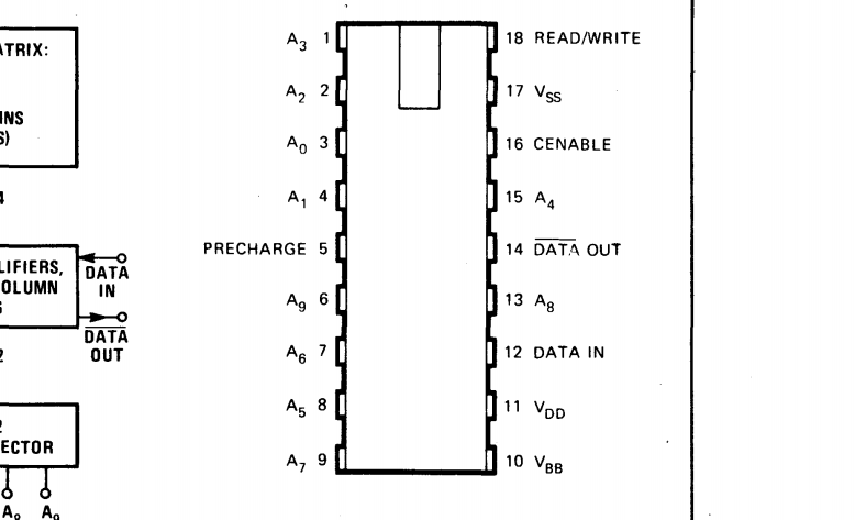
all these control and power rails required an expensive 18-pin package which contributed a lot to the final cost of the device.
but 3 years later (1973) a company called Mostek came along with the MK4096. this was the first *cheap* 4K-bit DRAM, and it used a very clever trick: notice there are only 6 address pins? 2^6=64, so what gives? the trick is RAS and CAS...

RAS and CAS stand for Row Address Strobe and Column Address Strobe (a strobe is a type of clock). by pulsing first RAS and then CAS, you can latch 12 bits of address, 6 bits at a time! this clever trick frees up a bunch of pins and let Mostek use a cheap 16-pin package!

the way it is implemented is that it feeds the row or column address into a decoder (for rows) and a mux (for columns). notice the sense amplifiers? there is one of them per column. when you address a row, the sense amplifiers automatically refresh that entire row.

basically, you access a row, and the sense amplifiers "refill the buckets" of all the bits in that row. so to refresh the entire memory array, you just have to pulse the RAS line for every possible 6-bit row address, and you're done.
as memory capacities increased, pins were sacrificed to make room for more address lines. the chip select line was somewhat redundant with the RAS and CAS, so that went away. semiconductor processes got better and so all the supply rails went away except for +5V.

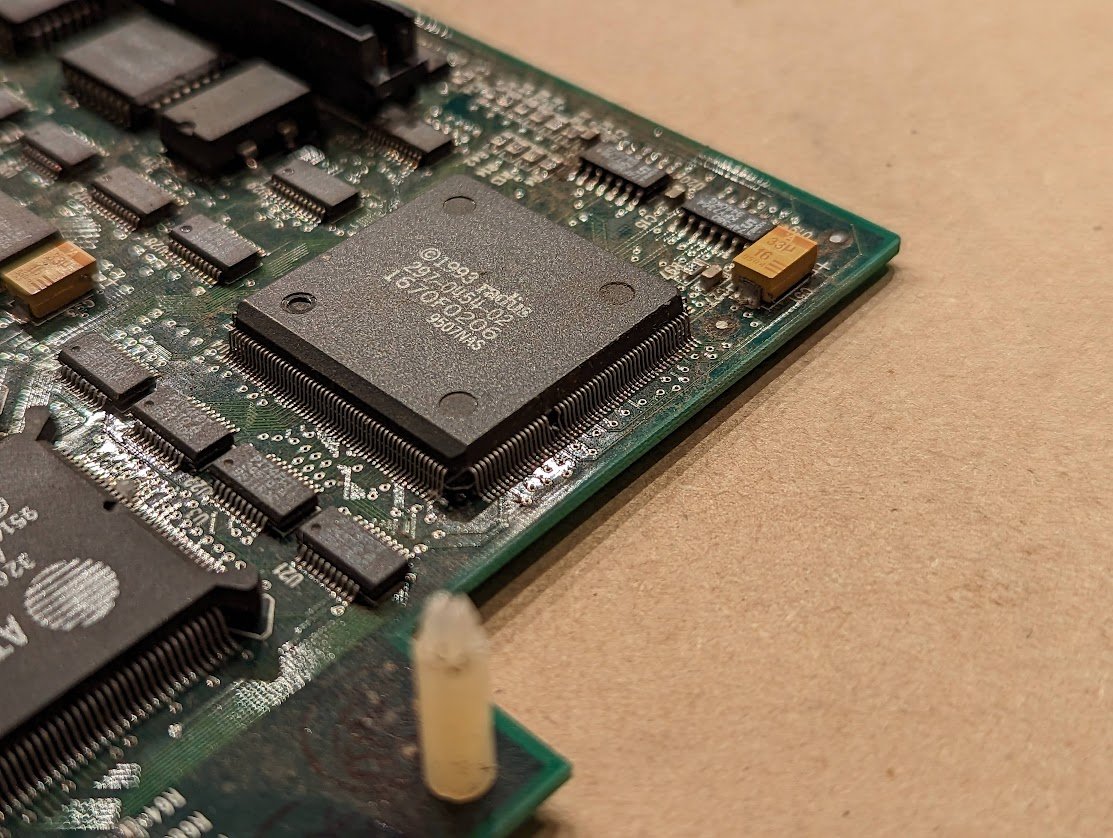
still later (late 80s, early 90s) when computers switched from DIP packaged parts to surface mount, other packages like this one became more common. the D (data input) and Q (data output) were combined into the same bidirectional pin, now called DQ. this chip has 4 of them.

then in 1993, a new type of DRAM became available: synchronous DRAM (SDRAM). this chip has a master clock, CLK. every operation is synchronized with this clock. the data path was widened to 8 bits, and some new pins crop up as well...

DQM (DQ mask): makes the data pins high impedance when asserted. this is used in 32-bit systems when you need to write to only 8 bits or 16 bits of a 32-bit wide memory system.
CKE is the clock enable. when the clock is disabled, the chip goes into a low power state.
this SDRAM also has a self-refresh mode: when you select RAS, CAS, then CKE, and then release CAS and CKE at the same time, the chip generates its own internal refresh cycle so you don't have to pulse RAS and supply all possible row addresses.
oh yeah, those control lines like RAS and CAS? they're not just for row and column select. various combinations of the control lines are now *commands* being sent to the SDRAM. this chip has some intelligence of its own!

another fancy trick is *burst mode* where the chip will read out (or write) several adjacent bytes given only one address. notice the delay between CAS loading a column address and the first data byte coming back? this is the *CAS latency* created by internal pipeline delays.

quick aside: some 16-bit wide SDRAMs start appearing in the 90s, and they have two separate DQM lines: UDQM and LDQM. if you only need to access the upper byte, then you assert the LDQM to mask off the lower byte.
hey, it's more convenient than doing a read-modify-write operation
hey, it's more convenient than doing a read-modify-write operation
now the RAM clock speeds are increasing, so signal integrity starts to become an issue. PC motherboard makers are starting to do some length matching of traces (to line up the electrical delay)
the voltages are going down as well, 3.3V is more common than 5V. most designs are using series termination resistors to help prevent excess overshoot and undershoot.
now we come to the year 2000, with the introduction of the DDR SDRAM (double data rate) 🎉
so many pins now!
so many pins now!

the biggest change is that data gets transferred on both the rising *and* the falling edges of the clock signal! each clock edge is called a "beat".

other changes:
✅CLK is now differential for improved signal integrity!
✅there are multiple *banks* of memory, accessible with bank select pins
✅each 8-bit data lane now has its own clock, called a "data strobe" or DQS pin
✅CLK is now differential for improved signal integrity!
✅there are multiple *banks* of memory, accessible with bank select pins
✅each 8-bit data lane now has its own clock, called a "data strobe" or DQS pin
data strobe? yes, during a write, you send a clock along with the data, and those PCB traces all have to be exactly the same length. during a read, the DDR chip *sends you* clock pulses on DQS along with the data you are reading! it is a bidirectional clock line.
other fun features: "2n prefetch" which means that the DRAM's internal data bus is twice as wide as the external data bus. when you read a word, the DRAM can immediately send you the next word because it's already read it!
DDR also introduced the concept of MT/s (million transactions per second). the original DDR spec ran up to 400MT/s, corresponding to a clock frequency of 200MHz (remember, it's doing a transaction on both clock edges!)
length match groups: traces that share a common clock line all need to be the same length. but they don't need to be matched with the lengths of traces that use a different clock.
DQ[n:0], DM, DQS are in one group per data lane
CK/CK#, A[n], BA[n], RAS#, CAS#, etc are in another
DQ[n:0], DM, DQS are in one group per data lane
CK/CK#, A[n], BA[n], RAS#, CAS#, etc are in another
DDR2 made further improvements:
✅lower voltage
✅higher speed (up to 1066MT/s)
✅4n prefetch
✅on-die termination (ODT)
and others
✅lower voltage
✅higher speed (up to 1066MT/s)
✅4n prefetch
✅on-die termination (ODT)
and others
ODT means that, for the bidirectional DQ bus, each chip (the DRAM or the controller chip) can switch on or switch off a termination resistor at each end.
DDR3 is even faster (2133MT/s), lower voltage (1.5V/1.35V), has 8n prefetch, and a few other changes BUT the most interesting change is the introduction of read and write leveling!
this is required because of the new "fly-by" topology for the address and control lines (green), which fly by each memory chip in sequence. it means that each chip sees the command at a slightly different time, and therefore the data comes back at a different time!

to compensate for this, the DDR memory controller has delay lines that it uses to slow down the signals coming back from nearby RAM chips so that they match the signals coming back from more distant RAM chips.
here's what the timing delays might look like on a PCB. address/control always has a longer delay. during write, data would arrive *before* the command so you have to add a delay for each data lane.

*setting up* those delays is tricky, and the process is called leveling.
for write leveling, the DDR chip goes into a special mode where it samples CLK on the rising edge of DQS, and puts the value onto one of the DQ bits. the DDR controller slowly advances the delay line value until DQ changes state.
that's the fine tuning first stage. the result could still be off by multiples of the clock period, so the second stage computes the clock cycle delay. (only send one DQS pulse, see how long it takes for DQ to change)
so that's how you compensate for the delay during a *write* operation (sending data from the controller to the DDR chip). read leveling is a bit trickier, and is not actually spelled out in the JEDEC specification!
which means each IP vendor develops their own "secret sauce" method. some good, some bad.
the first part is read DQS gate training. the "gate" blocks DQS clock pulses from being received *unless* they fall within a particular window of time. the controller loads a specific pattern into the DRAM (since writes work) and reads it back, sweeping the gate opening around

typically there's an upper and lower limit for the read gate timing (beyond which the data is not valid), so the controller tries to center it.
next, the controller performs a read/write bit deskew. since each data bit *within* a data lane has slightly different trace lengths (they could be off by 10 mils or more!) it adjusts individual bit delay lines so that everything matches up.
finally, the controller does read/write eye centering where it tweaks the delay lines just slightly to compensate for inter-symbol interference: two 1s followed by a 0 has a different zero cross transition than a 0, a 1, and then a 0. typically it uses a pattern like 1100101011..

now for the really crazy part: after the delay lines have all been set up, the controller has to *continually adjust* them as temperature and supply voltage change! this is called VT compensation, and it compensates for the fact that the delay lines drift.
DDR4 is very similar to DDR3: basically it is faster and has an even lower supply voltage.
newer memory standards get even crazier! i hear rumors about things like data bus ECC and extended memory array ECC since the cells are small enough the probability of seeing data errors gets to be quite high!
i should add some pictures of the waveforms you see in modern DDR systems.
here's a measurement made at the DDR chip. the DQ is the data bit and the DQS is the strobe (clock) for that data lane. each burst is 8 beats, so it transfers 8 bits per data bit.

you have to use special solder-in probes right at the vias behind the DDR memory chips. otherwise the voltage waveform you'll see won't be useful.

if you like spending lots of money you can even get fancy analysis systems like this.

what amazes me is that, in reviewing the history of DRAM, you can see how it's been a continuous set of improvements made over the last 50 years. and yet some things stay the same: we still have address lines and RAS/CAS. 😂
• • •
Missing some Tweet in this thread? You can try to
force a refresh