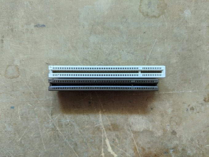
poking around inside an IBM PS/2 Model 80 from 1987, i noticed something odd going on with the expansion card connector. there are 8 extra pins in this connector, but why? the reason is really strange, and totally nuts!🧵 

but first--this bus connector is NOT a PCI connector, it is Micro Channel! in the picture, PCI is on the top and Micro Channel is on the bottom.
coming off of the success of the ISA bus used in the IBM PC, XT, and AT, engineers at IBM decided to "do it right" this time around.
the ISA bus, at first, ran at the CPU clock: 4.77MHz, and later 6MHz, 8MHz, 8.33MHz (the maximum!) and just about everything in between.
in addition, it had very poor signal integrity and the electrical design of ISA couldn't handle anything faster. (technical reasons? only 4 ground pins, no impedance control, and slow bus buffers)
so the IBM engineers went with a fancy connector (half the pin pitch!) and used 27 (!) ground pins, ground planes, better buffers, and so forth. signal integrity on Micro Channel (aka MCA) is pretty good.
confident in the new electrical design, the engineers set the clock speed of the bus at Ten Megahertz™. this was the official clock speed and it Could Not Be Changed.
the design was used in systems like the 10Mhz 286-based PS/2 model 50, in which the CPU matched the bus speed perfectly.
slow peripheral? no problem, there was a way to add wait states (extra clock cycles inserted in the bus cycle to slow it down temporarily while accessing that peripheral)
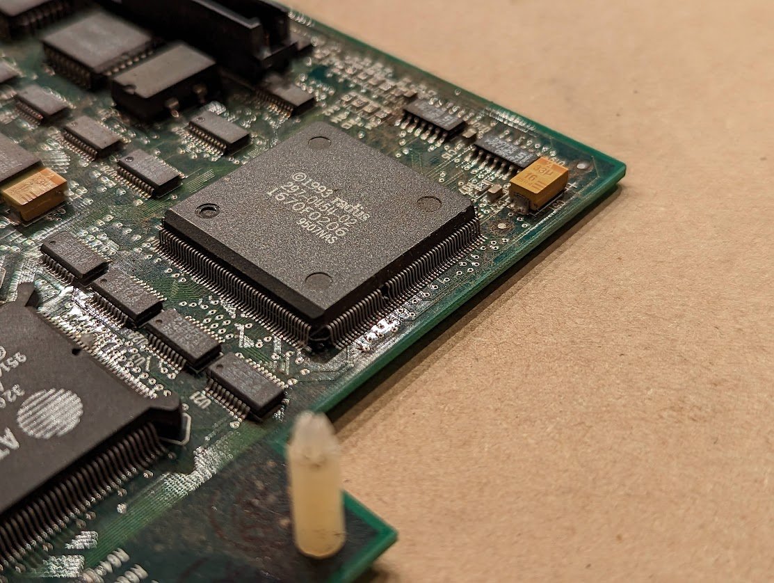
everything was really cool so far, but then Intel threw a wrench into the works. maybe you notice the issue already from just looking at this picture of a 386 chip.

the problem? the clock speed was...most decidedly inconvenient!
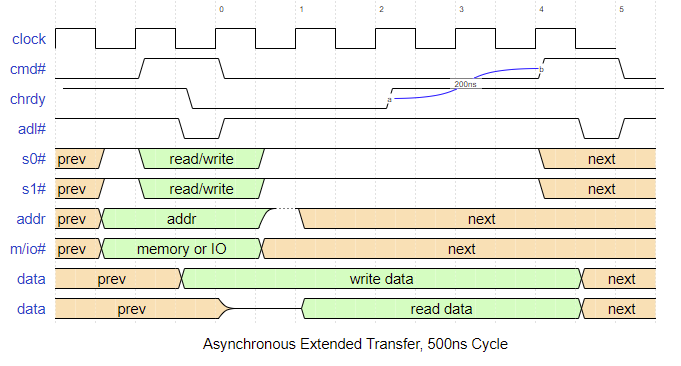
see, the basic bus cycle needed 200ns. that was the lower limit--set in stone--impossible to change. and you can't get 200ns with a clock of 16MHz!

IBM engineers faced an ugly choice:
1⃣ slow the fancy new 16MHz CPU down to 15MHz
2⃣ slow the bus down to a 250ns cycle
1⃣ slow the fancy new 16MHz CPU down to 15MHz
2⃣ slow the bus down to a 250ns cycle
1⃣ was not going to work. the industry would *laugh* at IBM trying to sell a 15MHz 386 computer. sure, it's about 6% slower which isn't too bad, but it just looks stupid!
2⃣ was not going to work either. the PS/2 model 50Z had zero-wait state memory at a 200ns cycle, and it was just a 286! a 250ns cycle meant that RAM accesses would be 20% slower. and that was just embarrassing.
but what if the bus cycle was set so that it was 3 CPU cycles, or 187.5ns? it's only 6.6% faster; why not just use it?
hear that? that's the sound of desperate engineers smacking into the inviolable brick wall called Ten Megahertz™: The Official Clock Speed That Shalt Not Be Changed.
i can imagine some poor IBM engineer stuck in a dingy conference room with a dozen colleagues, sweating through his white dress shirt and tugging nervously at his tie-constricted collar.
"guys, i have an idea, but you're not gonna like it"
what he proposed (and he was almost certainly male--this was IBM back in the 80s, after all) was a Really Ugly Hack
and it was such a Really Ugly Hack that everyone frowned in disgust, but realized that he was right, and that they had no other choice but to implement it.
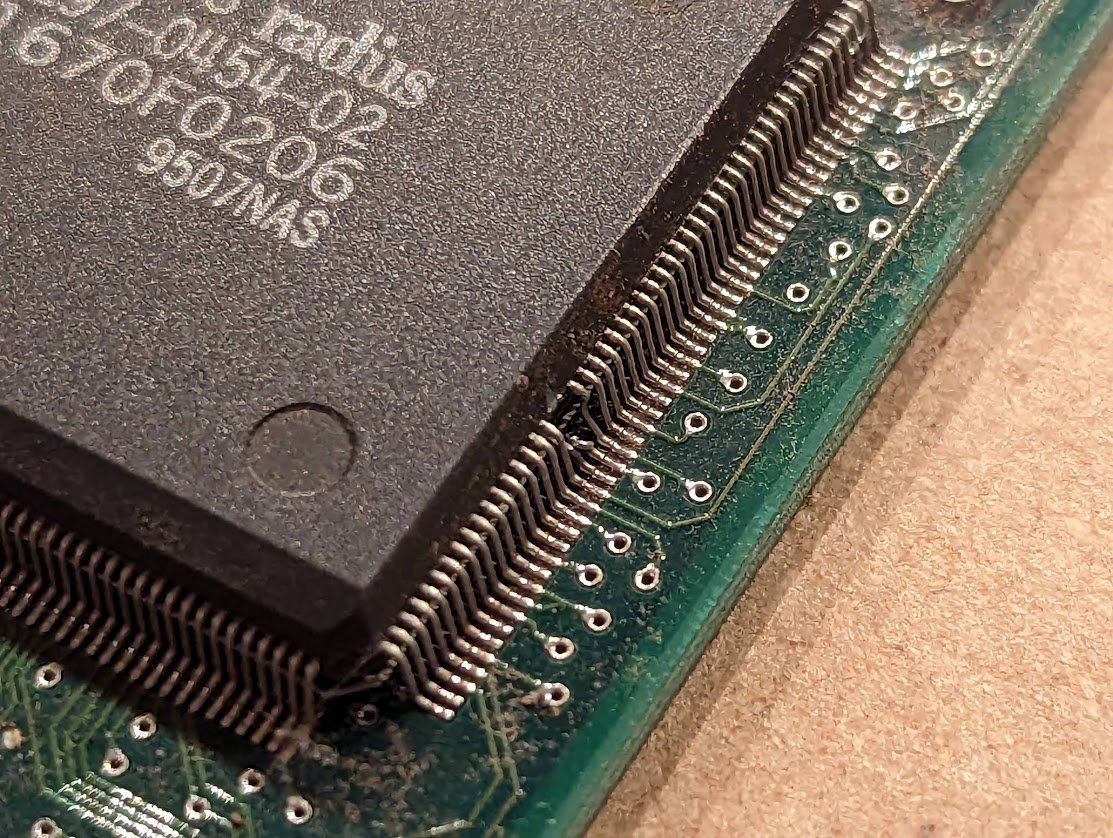
here's the Really Ugly Hack. they added 8 pins to the back of the bus connector, containing 2 ground pins (because why not) and three new signals implementing something called the Matched Memory Extension.

since the Ten Megahertz™ limit applied only to the existing bus control line CMD, they...
made...
a duplicate bus control line.
a duplicate that could run 6.6% faster.
made...
a duplicate bus control line.
a duplicate that could run 6.6% faster.
the other two lines were handshaking lines: the CPU controller asserted MMC to say "hey folks, i support matched memory cycles!" and a peripheral, like a RAM card, if it supported The Really Ugly Hack, would assert MMCR in response: "yes! i support it!"
then the CPU controller would start using MMC_CMD instead of regular CMD, and would run it *slightly faster* which beat the only alternative which was to run it *lots slower*
peripherals that didn't support MMC could just ignore the whole set of transfers because they only keyed off the CMD control line.
OK, the Really Ugly Hack is awful, but i haven't gotten to the worst part yet.
the PS/2 Model 80, which came out with the 16MHz 386, had two other variations: one at 20MHz and one at 25MHz. both those frequencies work perfectly with MCA.

and so these newer versions of the Model 80 had no need for the Really Ugly Hack. and with a slightly less ugly hack: the planar (IBM-speak for *motherboard*) asserts MMC during memory cycles, ignores MMCR, and drives the MMC_CMD line identically to the CMD line.
basically, it doesn't do anything.
oh yeah, let me tell you about the worst part!
the worst part is that the matched memory cycle, aka the Really Ugly Hack, was only ever implemented on the Type 1, 16Mhz planar of the PS/2 model 80.
and every MCA-based machine they built afterward had those connector pins.
and every MCA-based machine they built afterward had those connector pins.
now for the behind-the-scenes part! 😁
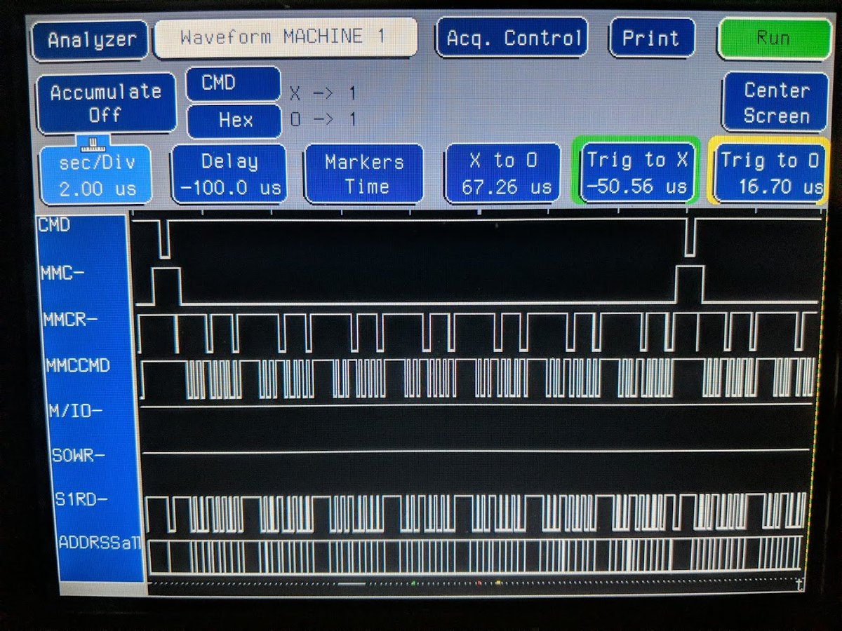
to get the logic analyzer plots, i used an old prototype Snark Barker MCA board. since i have connectors on it for logic analyzer probes, it made it really simple and easy!

the Snark Barker MCA doesn't need or use the matched memory extension, so i had to solder some wires (very carefully!) onto the memory card.

and then very carefully stuff it all back into the computer.

that reminds me. there's a funny thing i noticed as i was messing around with this project just now.
despite being a Type 1 planar/motherboard with a CPU clock of 16MHz, the CPU and math coprocessor are rated to...yeah. 20MHz. 🤦♂️

"sir, we ran out of 16MHz Intel CPUs, but we still have this huge pile of 16MHz motherboards! what do we do?"
"ship it with 20MHz CPUs! we got plenty of those!"
"ship it with 20MHz CPUs! we got plenty of those!"
oh yeah, and regular peripherals plugged into a 16MHz Model 80 met with this uber-slow 250ns bus cycle. that same peripheral, plugged into the 10MHz 286 Model 50 would run 25% faster 😂

oh yeah i need some credits. the first photo stars my Plaid Bib MCA-compatible Ad Lib card, with capacitors Snap and Crackle making a guest appearance.
(those familiar with the failure modes of tantalum capacitors AND 1980s breakfast cereal commercials will get the joke)
(those familiar with the failure modes of tantalum capacitors AND 1980s breakfast cereal commercials will get the joke)

the Plaid Bib MCA is open source, full design files available here: github.com/schlae/plaid-b…
i've also got an MCA version of my Snark Barker sound card clone. actually it's a bit unfair to call the MCA version a clone--i had to design the bus interface from scratch.
github.com/schlae/snark-b…
github.com/schlae/snark-b…

the nice timing diagram is from my Micro Channel bus tutorial, github.com/schlae/mca-tut…. it's for the discerning reader who wants to learn more about this fascinating bus before wondering why their head hurts, closes the browser tab, and exclaims, "it feels so good when i stop!"
and the diagrams themselves were created using the fabulous wavedrom.com
• • •
Missing some Tweet in this thread? You can try to
force a refresh