
Today's first #IEDM22 Short Course is HPC, Graphics, and Zettascale.
➡️ The Path to Zettascale, Intel
➡️ CMOS Scaling 1nm and Beyond, Samsung
➡️ Novel Logic Devices, TSMC
➡️ 3D Chiplets and Packaging, UCLA
➡️ Architecture for Power, imec
➡️ Optical Interconnects, Ayar Labs
➡️ The Path to Zettascale, Intel
➡️ CMOS Scaling 1nm and Beyond, Samsung
➡️ Novel Logic Devices, TSMC
➡️ 3D Chiplets and Packaging, UCLA
➡️ Architecture for Power, imec
➡️ Optical Interconnects, Ayar Labs
350 slides, this short course is going from 9am to 5pm. Not going to live blog, except certain parts.
For example, Wilfred Gomes of Intel outlines a deeper plan for Zettascale. In includes CryoCMOS discussions, i.e. running at 77K, although a ZF system is expected to be at ~0C
For example, Wilfred Gomes of Intel outlines a deeper plan for Zettascale. In includes CryoCMOS discussions, i.e. running at 77K, although a ZF system is expected to be at ~0C
The key to Intel's ZF (ZettaFLOP, 1ZF FP64 system), is the power. Trying to keep within the 40-100 MW per Supercomputer.
(Just noticed that Intel has changed the slide they're presenting to this one in the deck. The one showing says 16-32x ZettaOPs BF16.)
(Just noticed that Intel has changed the slide they're presenting to this one in the deck. The one showing says 16-32x ZettaOPs BF16.)

Intel's route to 1 ZettaFLOP of FP64 by 202X:
➡️ Arch: Falcon Shores+ (x86+GPU)
➡️ Software: OneAPI
➡️ Process: Stacked 2D Transistors
➡️ Packaging: Chiplet
➡️ Memory: 3D FeRAM as L2/L3
➡️ IO: Optical, Dragonfly
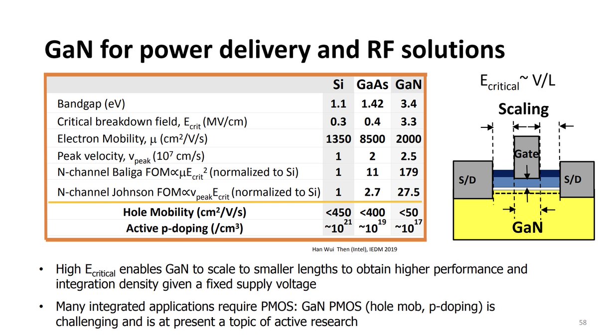
➡️ Power: HV IVR, ULV @ 355mV, GaN
➡️ Thermals: Chilled, CoolCMOS
➡️ Arch: Falcon Shores+ (x86+GPU)
➡️ Software: OneAPI
➡️ Process: Stacked 2D Transistors
➡️ Packaging: Chiplet
➡️ Memory: 3D FeRAM as L2/L3
➡️ IO: Optical, Dragonfly
➡️ Power: HV IVR, ULV @ 355mV, GaN
➡️ Thermals: Chilled, CoolCMOS


Note to people taking this tweet: Each one of these points is extremely nuanced. Slides only go into so much detail - there are talks on pretty much all of these segments that go into detail. LMK if you want a deeper explanation
A few more slides:
A few more slides:


What I enjoy is that when speaking about optical IO, Intel used their own chiplet packaging for external networking connect, but they used @LightmatterCo @theanalognick info for chip-on-wafer 2.5D packaging. Is this a tie-in, or just stating what's out there?

'If you reduce cache latency 10x, you can have caches 1/10th the size'.
Erm what?
Erm what?
Intel has III/IV internal optical lasers. The aim is to get down to 0.5 pJ/bit, there's currently a path to 1 pJ/bit.


Power use and the need for GaN and the right input voltage to get closer to 90% efficiency.


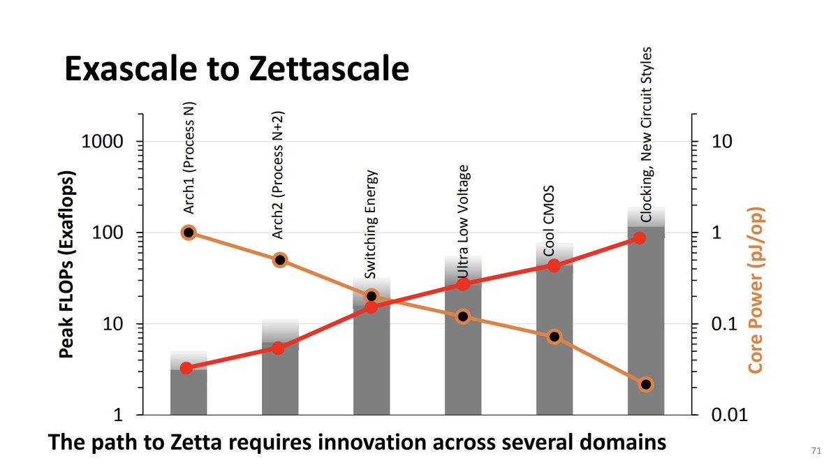
This graph is somewhat wild. I think he just said Arch1 was Ponte Vecchio - but it doesn't do 3EF/chip, so I have no idea. But look at that pJ/op orange line. Today, 100 pJ/Op. Down at the bottom, that's 0.02 pJ/Op - a 5000x reduction in energy per operation needed.
On this slide.
They're quoting 3.2 MW for interconnect. Simply for interconnect!
Also, tiles and groups. He just said these aren't individual chips, so I think we're looking at that tile based integration, like Dojo or using a Lightmatter or similar solution.
They're quoting 3.2 MW for interconnect. Simply for interconnect!
Also, tiles and groups. He just said these aren't individual chips, so I think we're looking at that tile based integration, like Dojo or using a Lightmatter or similar solution.

Got up to ask about whether Intel is developing its own interposer/wafer optical networking solution or if they're working with @LightmatterCo . Wilfred said that it's more of an open question really - the industry hasn't embraced chiplet photonics yet /1
2/ The benefits of chip-to-chip photonics vs electrical haven't been realized yet, which is half the problem. (I suspect it's also cost-related right now.) But there are going to be solutions that use one, the other, or both. Probably.
He just mentioned Vertical 2D transistors. That would be hard to manufacture I bet!
No-one was asking questions, so I asked another. He mentioned the 355mV ultra low voltage blockchain ASIC, so I mentioned how applicable is that to HPC for Zettascale.
/1
/1
2/
Wilfred said that half the issue is the way compute is being done today. Holding states has to go, and moving to async clocks. It's also all about the test and design. HPC is moving this direction anyway, so the work is being done today. Blockchain ASIC was the start.
Wilfred said that half the issue is the way compute is being done today. Holding states has to go, and moving to async clocks. It's also all about the test and design. HPC is moving this direction anyway, so the work is being done today. Blockchain ASIC was the start.
Wilfred just said that the external laser connections into the chip, he thinks it'll never work (despite Intel showcasing it back at Innovation a couple months back!!).
He's more of an advocate for a table-sized chip where everything is on package. (So, Tesla?).
He's more of an advocate for a table-sized chip where everything is on package. (So, Tesla?).
Next talk is Samsung, about technologies to scale to 1nm nodes. The big thing here is Samsung's name for CFETs: 3DS FETs. Showcasing vs MBCGET (what Samsung calls GAA)
➡️ 50% logic area saving
➡️ 43-50% SRAM area saving
If you're stacking it, of course you half the area 🙃
➡️ 50% logic area saving
➡️ 43-50% SRAM area saving
If you're stacking it, of course you half the area 🙃

*MBCFET, obviously. I always forget if it's MBC or MCB. But this error is new
But future scaling to 1nm has to come from:
Contact Poly Pitch (CDD)
Cell Height (sheet pitch, M1 pitch)
CPP x Cell Height is your cell area. Can work on both separately. Kinda.
Contact Poly Pitch (CDD)
Cell Height (sheet pitch, M1 pitch)
CPP x Cell Height is your cell area. Can work on both separately. Kinda.

But Stacked Transistors have many problems, let alone just getting the scaling. Manufacturing has to change - are you sequential or monolithic? Will the temperature of a step cause a degradation of the NMOS/PMOS you've already built etc?


Sequential means stacked - using two wafers and bonding them, which requires packaging technology.
Monolithic means building it into the silicon one after the other, which needs high aspect ratio design and low temp process steps.
Monolithic means building it into the silicon one after the other, which needs high aspect ratio design and low temp process steps.


To correct myself - I thought the demo Intel showed at Innovation was a laser going into the chip. It was actually the laser going out. Wilfred was stating that with the laser on the chip, that's the only solution that'll work, and that's what was shown. My bad! Sorry about that.
• • •
Missing some Tweet in this thread? You can try to
force a refresh


