The Intel 8086 processor was introduced in 1978, ancestor of the x86 architecture. The 8086 was the first microprocessor with prefetch, reading instructions from memory in advance for more speed. By reverse-engineering the chip under a microscope, I can explain how this works. 🧵
The 8086 has a 6-byte prefetch queue (photo), which is tiny compared to the megabytes of cache on modern processors, but it increased performance by about 50%. Intel ran a bunch of simulations to decide on the 6-byte queue (4-byte on the 8088 with its narrower 8-bit bus).
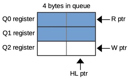
The prefetch queue was managed by a read pointer and a write pointer that kept track of the words in the queue. These 2-bit counters cycled 0-2. The HL flip flop indicated the high or low byte. The MT (empty) flip-flop indicated that the queue was empty.
This diagram zooms in on the prefetch pointers and associated logic on the die. This circuitry takes up a significant chunk of the die.
A processor's program counter or instruction pointer (IP) keeps track of what instruction it will execute. But prefetching moves the IP ahead of its "real" value. Subtracting the queue length gets the "real" IP. A Constant ROM holds constants -1 to -6 for this correction.
The interface between prefetching and the microcode engine was the "loader". This state machine fetched the first two bytes of the instruction from the queue. It also let microcode start the next instruction a cycle before the current one ended by pipelining decoding.
Prefetching added a lot of complications to the memory control circuitry since prefetches and "regular" memory accesses both needed to use the bus and needed to avoid conflict. My blog post has more information on how 8086 prefetching works: righto.com/2023/01/inside…
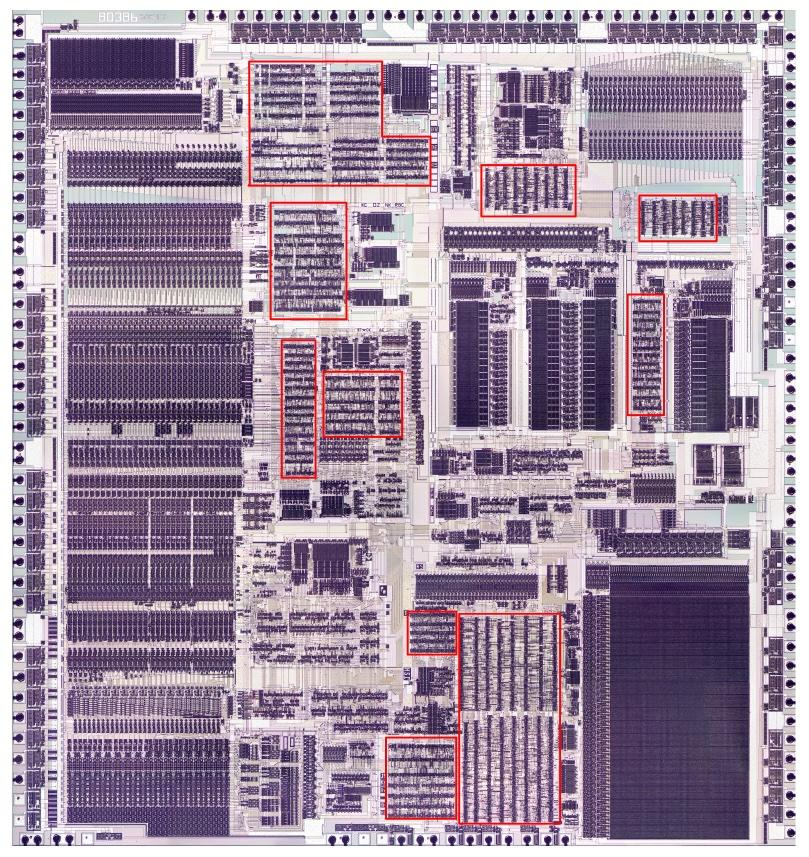
The Intel 386 processor (1985) was a key step in the evolution of x86, moving to 32 bits as well as a CMOS implementation. A less visible design change is its use of standard cell logic (marked in red), building many circuits from standardized building blocks. 1/17
The 386 was originally scheduled for 50 person-years of development time, but it fell behind schedule. The designers made a risky decision to use "automatic place and route", letting software do some layout. This worked and the chip was completed ahead of schedule. 2/17
Early chips had every transistor drawn by hand. Federico Faggin, designer of the popular Z80 processor (1976), spent three weeks drawing transistors but the last few transistors wouldn't fit so he had to erase everything and start over. The result was dense and chaotic. 3/17
The Intel 8086 processor (1978) started the PC era and most desktop computers still use the x86 architecture. Its instruction set is complicated with a variety of formats. This made decoding each instruction a challenge. The Group Decode ROM was a key part. 🧵
Most 8086 instructions are implemented in microcode, a level of instructions below the familiar machine instructions. But before microcode can run, something called the Group Decode ROM categorizes instructions according to their structure, shown as colors below.
The Group Decode ROM generates 15 signals indicating how to decode the instruction. For instance, can it run without microcode? Does it have bits specifying the argument size? Is it followed by an addressing (Mod R/M) byte? Then the processor executes the instruction.
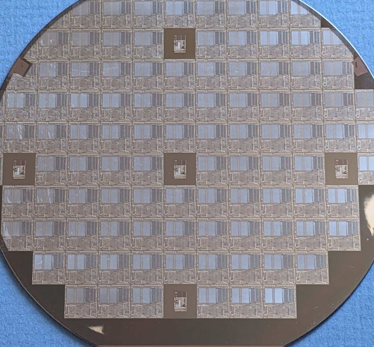
Here's a silicon wafer for Intel's iAPX 432 processor (1981), a failed "micro-mainframe". Each rectangle on the wafer is one processor chip. But what are those five unusual rectangles? Those are test circuits... 🧵
Creating chips on a silicon wafer is complicated and lots can go wrong. A few test circuits were placed on the die so Intel could check the important characteristics and make sure everything was okay. The white squares are test pads. Tiny probes contact the pads for measurements.
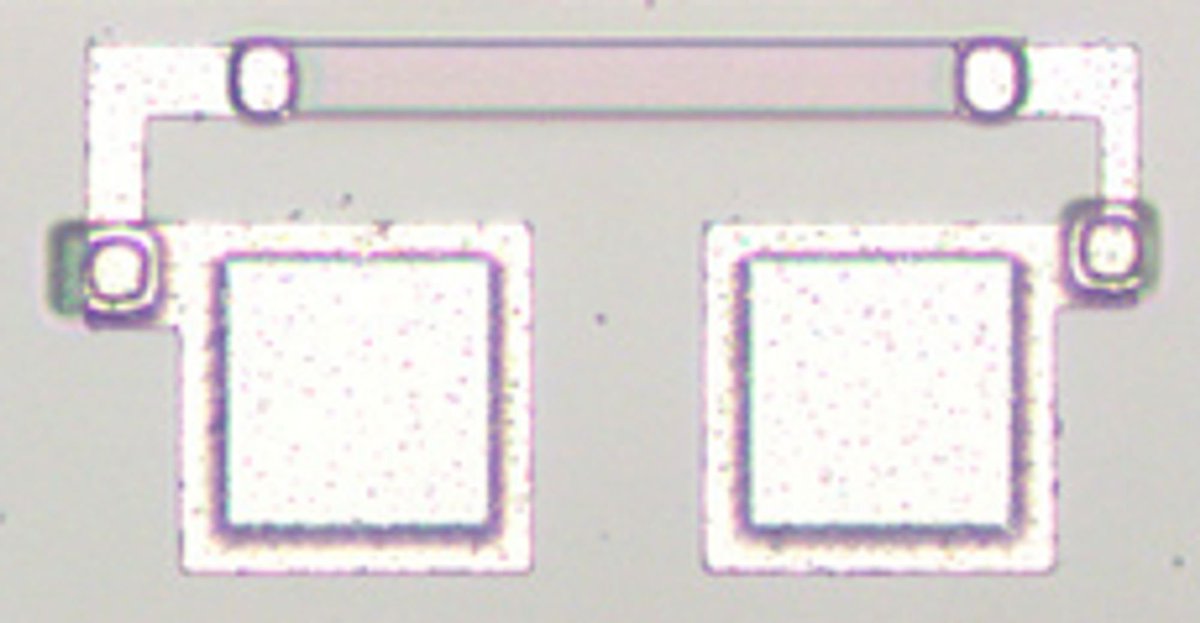
For instance, these two test circuits were used to check the resistance of materials on the chip. The long rectangles are the regions to test and they are connected to the metal test pads. If the resistance is wrong, the manufacturing process can be adjusted.
This Central Air Data Computer (CADC) was introduced in 1955. It computed airspeed, altitude, etc for fighter planes. But instead of a processor, it was an analog computer that used tiny gears for its computations. Let's look at how one of its modules works.🧵
Planes determine altitude and speed from air pressure readings. But near the speed of sound, things become very nonlinear. As fighter planes became supersonic in the 1950s, the CADC was built to compute these nonlinear functions using rotations of gears and cams.
The CADC needs to know the temperature for its calculations. A platinum probe outside the plane measures temperature, producing a changing resistance. But the CADC needs to rotate gears. How does the CADC convert the resistance to a rotation? That's what I'll discuss today.
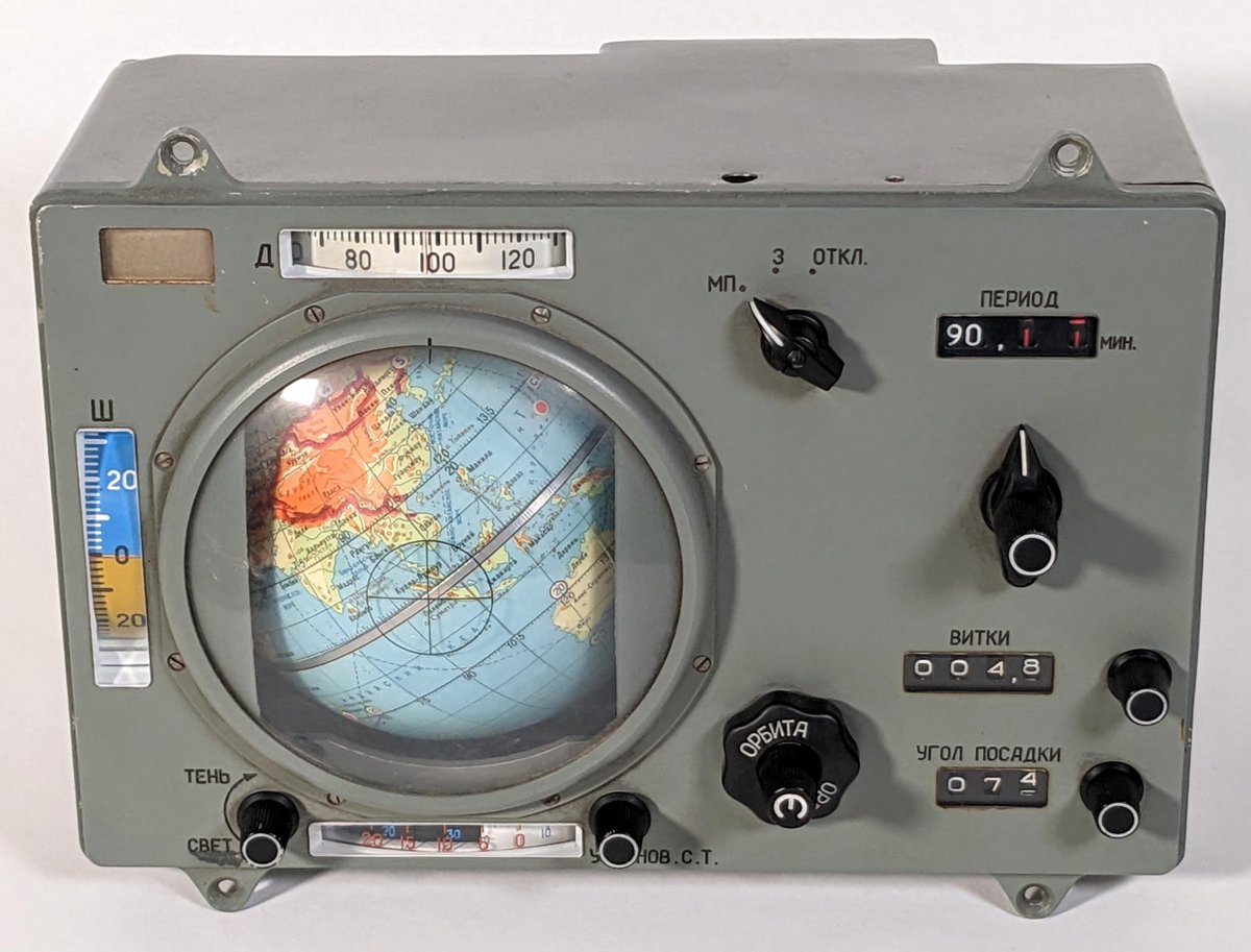
Soviet cosmonauts used the Globus INK to track their position above the Earth. In use from 1967 into the 21st century, the Globus is an analog computer, crammed full of tiny gears. I reverse-engineered the Globus and can explain how these gears compute the orbit. 🧵
The key component is a differential gear assembly that adds two rotations. Three spur gears provide two inputs and an output, while the spider gear assembly spins to generate the sum. The differential in your car uses a similar principle.
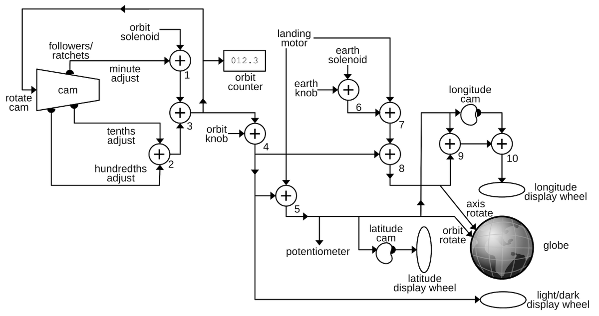
I made this diagram to show how rotational signals travel through the Globus. The ten differentials "⨁" add signals while three cams implement complicated functions. The results turn the globe and other indicators.
Intel introduced the 8086 microprocessor in 1978 and it still has a huge influence through the modern x86 architecture used today. This 16-bit processor contains a bunch of registers, some of them hidden. I reverse-engineered the 5-bit code that it uses to select registers. 🧵
Instructions for the 8086 processor specify registers through 3 bits in the opcode or following byte. This is expanded to a 5-bit code to support 16-bit registers (red), 8-bit registers (blue), segment registers (green), and special internal registers.
To provide a level of indirection, the 5-bit register specifications are held in the internal M and N registers. This closeup die photo shows how the M and N registers are implemented on the chip.