What’s inside Apple’s $129 Thunderbolt cable? We CT scanned one to find out, and compared it to some cheaper cables… 🧵
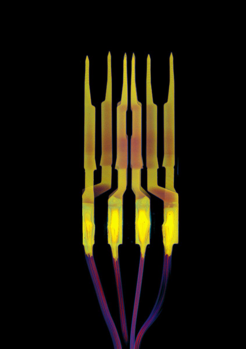
Turns out there’s a lot going on in this Thunderbolt 4 connector. There’s a very complex PCBA that appears to have two inductors. This cable can deliver 100W to the connected device, plus it has to power its own ICs. 

The PCBA has 9 layers, with lots of blind and buried vias. An industrial CT scan lets us filter by density; in the second image, I’ve removed the PCB substrate from the visualization, showing the denser materials in the vias.


Data can flow through this connector so fast that microscopic differences in trace lengths matter. Notice how the inside trace in this pair has a wiggle that makes it exactly as long as its outer counterpart.

The cable is a work of art. 20 separate wires, 10 of them coaxially shielded. The wires and their shields are soldered to the PCBA separately. It’s all protected by a strain-relief fitting that’s crimped in from 8 directions.


The wires that transmit power are soldered together upon reaching the PCBA; the data wires are soldered independently. This is very high-quality soldering, but even Apple’s solder has a little bit of porosity.


Here’s another fun animation before we move on to some other connectors.
By the way, you can explore these scans for yourself here:
lumafield.com/article/usb-c-…
lumafield.com/article/usb-c-…
Here’s an Amazon Basics USB-C connector. It’s thoughtfully designed, though without any of the intricacy that we see in the Thunderbolt connector.
While the Thunderbolt connector has all 24 pins allowed by the USB-C standard, this connector has just 12 pins, and they’re not independently connected to the PCBA; where mirrored pins are present, they’re jumped across.

@lumafield While the Thunderbolt’s PCBA is bristling with surface-mount components, this has none. The PCBA in the Amazon Basics connector just connects pins to wires. The strain relief here is much simpler than the Thunderbolt’s, too: it’s just a pair of arms crimped together.


@lumafield This cable is fairly complex, though; it has 5 wires, two of which have hollow cores. And the whole thing is shielded by woven wires that land at the connector’s metal enclosure. Way better than what we’re about to see…

@lumafield Now for the extreme comparison. This is a $5.59 USB-C cable offered by NiceTQ. It went off the market immediately after I ordered it.
Nothing here is shielded; the pins and the connector’s shell are all floating independently in overmolded plastic (along with a splatter of metal inclusions left over from the soldering process).

There are 8 pins in this connector, but only 4 are connected to anything at all, soldered directly to the cable’s wires. The other 4 are floating in overmolded plastic along with the connector’s shell.
The listing for this cable claims it transfers data at 10 Gbps. That would be a USB 3.1 Gen 2 speed, but its pins and wires are only configured for USB 2.0, which maxes out at 480 Mbps. There's no redundancy; if one of the four active pins wears or breaks, this will stop working.
Compared to the other cables we’ve looked at, this one is very simple: 4 stranded wires with rubber insulation and no shielding.

Here’s a mystery: an even cheaper cable (just $3.89) that has a much more complex design. This one is by ATYFUER and only claims to transmit power, not transfer data.
This connector has all 24 pins, each individually fixed to a PCBA–a construction detail that’s present in the $129 Apple cable but not the $10 Amazon Basics cable. Only 12 of those pins are connected to traces on the PCBA, though (5 on one side, 7 on the other).

The PCBA connects those 12 pins to just 4 wires, which are soldered on with quite a bit of porosity. Why have 24 pins if only 12 are connected? Why not economize by having fewer pins, like the Amazon Basics connector?

My guess is that this factory also makes a Thunderbolt cable, and it’s cheaper to maintain a single design and process for the pin assembly, even though that means more material and more components. If you know why it’d be designed this way, reply to the thread!
Although this is only advertised as a charging cable, it’s configured as a USB 2.0 cable that can transmit data, with two thicker stranded wires for power about 0.75mm in diameter (~AWG 20) and two thinner wires for data about 0.4mm in diameter (~AWG 26).

CT scans show relative material density; the blue color in the scan shows that the power wires are less dense–probably aluminum–and the yellow data wires are denser, probably copper. How much money is this manufacturer saving by mixing aluminum and copper?

You can explore these scans yourself! This post has links to each scan; if you're on a computer you can slice through them and play with relative densities just like I've done above. lumafield.com/article/usb-c-…
This thread was made possible by my engineering colleagues at @lumafield, who were able to glance at these scans and find interesting details. If that sounds fun to you, check out our open positions here: lumafield.com/careers
@lumafield If you’ve made it this far, you might enjoy this introduction to industrial CT!
• • •
Missing some Tweet in this thread? You can try to
force a refresh