This is a CT scan of Heinz’s new ketchup cap. It represents a $1.2 million engineering investment over 8 years. Here’s why it’s significant… 🧵
This is the previous Heinz cap design. CT scans like @lumafield’s capture density, shown here on a blue-red spectrum. There are three plastics in this cross-section. The bottle is PET, and the cap is unlabeled but likely polypropylene. Inside the cap is another material. 
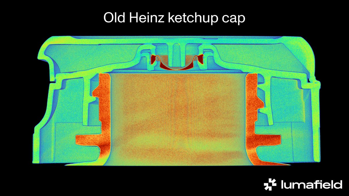
@lumafield @HeinzTweets @KraftHeinzCo @BerryGlobalInc It's a small silicone valve. Here we strip out low-density plastic (the PP cap) and isolate the PET body and the silicone valve. Silicone is flexible and durable, and the design of the valve lets ketchup pass at a predictable rate when the bottle is squeezed.
@lumafield @HeinzTweets @KraftHeinzCo @BerryGlobalInc The silicone valve embedded in the polypropylene cap makes it impossible to recycle the cap. Finding a mono-material cap design that could perform as well as the silicone was an enormous engineering challenge.
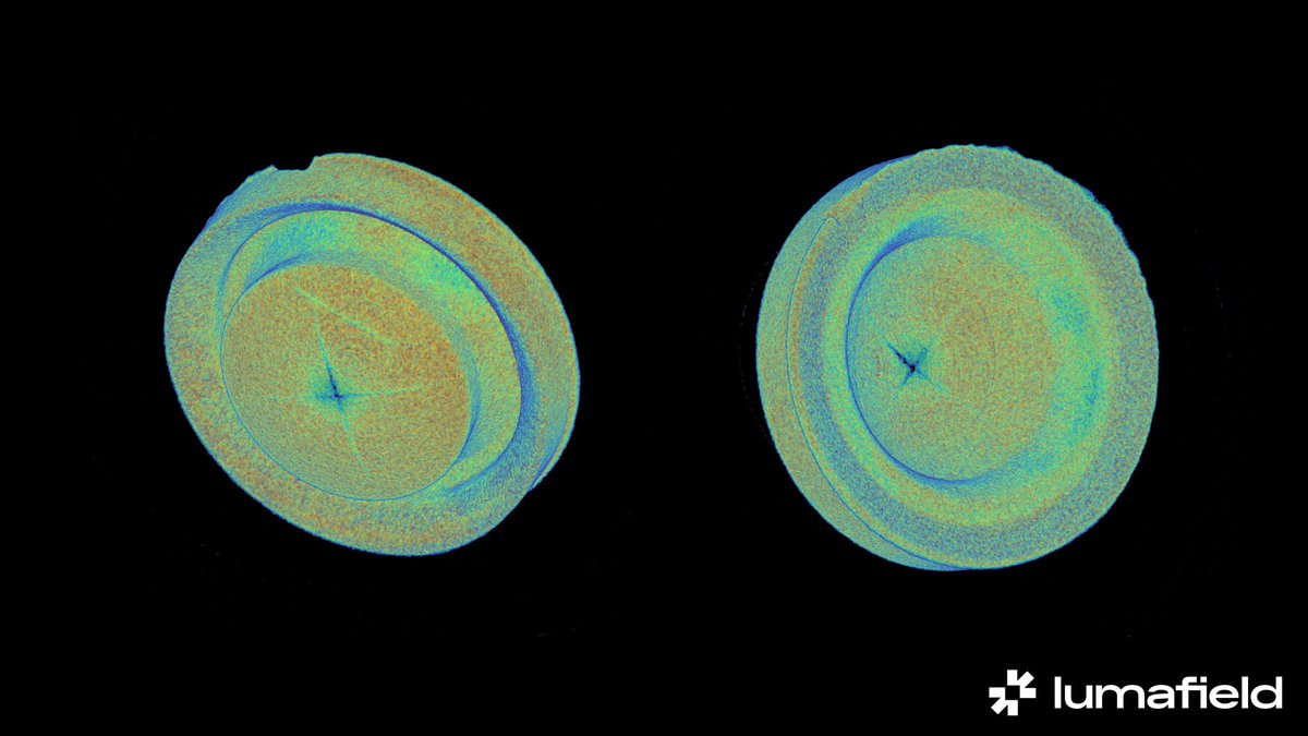
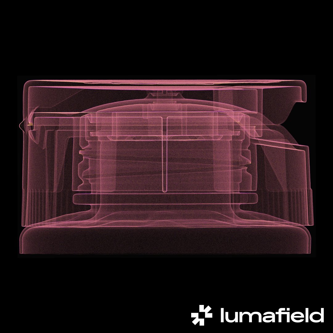
@lumafield @HeinzTweets @KraftHeinzCo @BerryGlobalInc Here’s Heinz’s new, fully recyclable ketchup cap. It’s made of polypropylene and doesn’t use a silicone valve. You can explore the scan right here! lumafield.com/article/heinzs…
The silicone valve is replaced by a complex set of channels and an antechamber inside the cap. Ketchup is a shear-thinning fluid that becomes less viscous as it’s deformed. A firm squeeze of the bottle forces ketchup through these channels, where it becomes thinner and dispenses at the familiar, predictable rate.

@lumafield @HeinzTweets @KraftHeinzCo @BerryGlobalInc Heinz's 8-year, $1.2M engineering investment with @BerryGlobalInc, which produces the new packaging, is a good–if extreme–example of what it takes to develop sustainable plastic packaging. This is an incredibly complex design, with a lot of underlying physics.

@lumafield @HeinzTweets @KraftHeinzCo @BerryGlobalInc Recyclable plastic can’t just be substituted directly for non-recyclable plastic; even small changes in polymer characteristics have a big effect on product performance. In the case of packaging, that means leaks and breakage that can cause lots of waste.
@lumafield @HeinzTweets @KraftHeinzCo @BerryGlobalInc Developing sustainable packaging is a giant engineering and manufacturing challenge that often involves comprehensive redesigns. You can learn about this challenge–and explore our CT scan of the new Heinz cap, here: lumafield.com/article/heinzs…
• • •
Missing some Tweet in this thread? You can try to
force a refresh