
I implemented an LLM end-to-end in hardware, and ran it on an FPGA.
Zero Python. Zero CUDA. Just pure SysVerilog.
All my progress + everything I learned from 200h of LLM chip design (demo at the end)👇
Zero Python. Zero CUDA. Just pure SysVerilog.
All my progress + everything I learned from 200h of LLM chip design (demo at the end)👇

Before we dive into the project log, some context:
I made this as part of a lab project for the most cracked course at Waterloo: ECE 327. Nachiket Kapre (the Prof) designed this lab.
Because of it, I went from knowing ZERO Verilog to now squashing delta‑cycle races caused by #0 delays in fork/join_any constructs.
I thought this lab is so goated that I'd make a detailed thread describing how anyone with some RTL skills could build this from absolute scratch (including deciding on the architecture / model support itself).
DISCLAIMER: this thread will be detailed and likely not make sense for those with zero RTL experience.
Phase 0: Learning system verilog
To implement anything in hw, you need to know a hardware description language (HDL). Since the course used system verilog, I got cracking on hdlbits.01xz.net
Hdlbits taught me the core syntax & structure of verilog:
• What is a module and how to define it (module ... endmodule).
• Input/output/inout port declaration (input, output, inout).
• Data types (logic, parameter, integer).
• Basic assignment (assign for combinational, = blocking, <= non-blocking for sequential).
And then to understand the general software pattern for digital design, I had to understand:
• Behavioral & Structural Modeling: always blocks (especially @(posedge clk) for synchronous logic). Understanding blocking vs. non-blocking assignments in sequential circuits. Module instantiation (connecting ports by name or order). Hierarchical design (modules within modules).
• Synchronous Design: Designing logic triggered by a clock edge. Understanding registers and flip-flops (how they are inferred).
• Combinational Logic: Designing logic without clock dependencies.
This process gave me a good high level understanding of verilog, but to complete this lab I needed to know these crucial techniques:
• Finite State Machine (FSM) design (state registers, next-state logic, output logic).
• Pipelining concepts (inserting registers to break critical paths).
• Working with vectors/arrays (e.g., logic [N-1:0] data;, connecting to array ports).
• Basic simulation constructs ($display, understanding testbench structure).
• Grasping how signal bundles (like AXI streams with tvalid/tready/tdata/tlast) work for handshaking, even if only connecting pre-made interfaces.
Essentially, a solid foundation in digital logic design principles implemented using Verilog syntax and common structural/behavioral modeling techniques proved essential.

Phase 1: Making high-level model arch decisions - BERT transformer + int quantization
To ensure the transformer weights fit on the FPGA and are edge-friendly, the Prof chose to focus on building the chip for the I-BERT architecture. BERT is one of the first large transformers and the 'I' means it's end-to-end quantized on INT8 (reducing memory footprint).
Making this decision required:
• Studying the standard floating-point BERT/LLM attention mechanism.
• Researching and selecting integer quantization techniques (like those in the I-BERT paper). This involves choosing fixed-point representations or integer approximations for all operations.
• Adapting algorithms like Softmax, GELU, and Layer Normalization to use integer-only math (this was done in
arxiv.org/pdf/2101.01321).
• Defining the exact mathematical operations, intermediate data types (bit widths like 8b, 16b, 32b, 64b), and precision requirements for each step shown in the diagram (e.g., the requant steps). This means implementing python functions that produce the bit-matching expected outputs for each set of expected inputs.
, Prof Nachiket Kapre IBERT py system diagram](https://pbs.twimg.com/media/GqHKAZEWcAEWMtV.jpg)
Phase 1.5: Choosing the systolic array microarchitecture (Google's TPU architecture) + AXI communication interface
With the model architecture and algorithms ironed out, we can decide on a compatible hardware architecture:
• Core acceleration strategy: we chose a systolic array microarchitecture for matrix multiplication due to its efficiency on FPGAs.
• Memory Strategy: we need to determine how large matrices (weights W, intermediate results Q, K, V, S, P, C) will be stored (likely external RAM banks on the FPGA) and how they will be accessed. Also needing to plan for data partitioning across memory banks.
• Interface Definition: we must choose standard interfaces for communication between modules (AXI Stream for high-throughput data, AXI Lite for control/configuration).
This phase was already completed for me since the prof had made these high level architectural decisions to ensure the design was tractable within a semester.
](https://pbs.twimg.com/media/GqHJ8UuW0AAVFx2.png)
Phase 2 (70% of the work): Implementing core computations in verilog
Now that I know the exact algorithms the hardware is supposed to implement, I need to translate this functionality into functionally equivalent verilog modules:
1. Basic Arithmetic Blocks:
-> Designed and implemented the fundamental Verilog modules: acc, mac, max, div, exp, gelu, sqrt.
-> Developed thorough Verilog testbenches (_tb.sv) for each, comparing outputs against Python reference implementations (.py) from the previous phase. Perform rigorous functional simulation (e.g., using Xilinx Simulator xsim or Verilator).
2. Systolic Array:
-> Designed the Processing Element (pe.sv), focusing on the MAC operation and data forwarding logic. Test it thoroughly.
-> Designed the systolic.sv module, using Verilog generate statements to create the N1xN2 grid and wire the PEs together, handling input injection and result shifting. Created a specific testbench for the systolic array, feeding it matrix data and verifying the output against numpy.matmul. Simulate extensively.
3. Transformer block primitives (softmax, layer_norm):
-> Designed softmax.sv and layer_norm.sv, integrating the primitive modules from step 1. Crucially, design the necessary buffering (e.g., using sreg.sv or fifo.sv) to handle latency differences between pipelined blocks (exp) and multi-cycle/reduction blocks (max, acc, div, sqrt). Developed testbenches and simulate, comparing against Python reference implementations again.
Having a waveform analysis tool and $display monitor was crucial to solving a bunch of nasty bugs during this stage. Once all functional tests pass, I was sure that the verilog modules were equivalent to the python kernels assuming zero wire propagation delays.

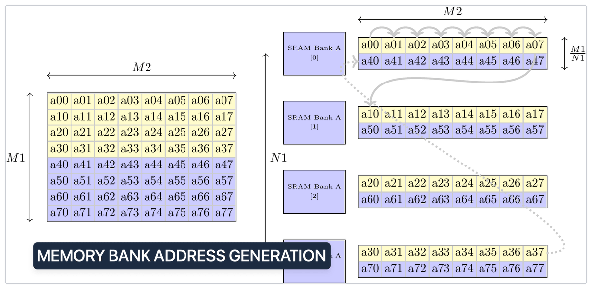
Phase 3: Implementing the memory controllers/address generators + AXI interface modules
With the computational verilog kernels complete, the memory modules are left. This is the infrastructure enabling smooth data movement between modules and memory banks.
1. Memory Interface Logic Tasks:
-> Design the memory bank wrappers
-> Design the address generators for the systolic array (mem_write_A, mem_write_B, mem_read_D). This is complex, involving cascaded counters to handle matrix partitioning and data interleaving/permuting. Getting these right requires standalone tests and really understanding the data layouts.
2. AXI Interface Modules Tasks:
-> Define or adopt standard AXI Stream interface definitions (axi_stream_if.sv).
-> Develop modules to bridge between memory banks and AXI streams (s2mm.sv - Stream to Memory Map, mm2s.sv - Memory Map to Stream). These handle the handshaking and data packing/unpacking.
3. Control Logic Tasks:
-> Design top-level control FSMs or logic (control.sv, attn_head_fsm.sv) to manage the overall flow: loading weights/biases, starting computations in sequence, handling valid/ready signals between stages.
Phase 4: Stitching everything together (top-level assembly)
With all of the core verilog modules built, now comes stitching them together into higher level usable modules like mm (matmul), mm_gelu (matmul gelu fusion), attn_head (full self attention computation), and then instantiating these higher level modules to define the chip layout with necessary clock generators.
1. Sub-System Assembly:
-> Create wrapper modules like mm.sv (combining systolic with memory interfaces and address generators), mm_ln.sv (combining mm, requant, mat_add, layer_norm_top), mm_gelu.sv (combining mm, requant, gelu_top), attn_head.sv (integrating multiple mm instances, requant, softmax_top, concat).
-> Connect these sub-systems using the defined AXI interfaces. Pay close attention to matching data widths and AXI signal connections (tdata, tvalid, tready, tlast).
2. Top-Level Verilog Design (ibert_axi.v / _on_axis.v):
-> Instantiate all the major sub-systems (attn_head, mm_ln, mm_gelu, etc., depending on the final target).
-> Instantiate clock generators, reset logic.
3. Constraint Files (clock.xdc): Define clock frequencies and pin assignments for the target PYNQ board.

Phase 5: Design verification (Synthesis + Post-Implementation simulations)
Even though this is the last phase, in actual development, testing and design verification is done alongside developing each module. It's the most important stage to verify your HDL performs as expected.
Here's what design verification means:
- After writing the verilog for a module, you (1) synthesize it which means you generate a circuit of gates (from an available set of primitives), and then (2) you implement it which means you place and route these gates on a die or in the case of an FPGA you lay out the LUTs and DSPs physically on the chip.
- After each stage, a new granularity of testing is unlocked: (1) functional verification is the fastest simulation and it checks that you're generating the correct waveforms by running the verilog module assuming zero propagation delay, (2) synthesis verification tests that you're simulation waveforms match expected once you account for the delay models of each gate/component, and (3) post-implementation simulation is the slowest simulation of the final netlist after place-and-route which simulates the entire chip including gate/component + routing delays.
So this is the workflow I had to go through for doing DV in this project:
1. Code Check (Lint): Catching Verilog errors early.
2. Basic Logic Check (Functional Simulation): Does it do the right math?
3. Hardware Translation Check (Synthesis/Implementation): Does it map correctly to the FPGA?
4. Post-Hardware Mapping Check (Post-Synth/Impl Simulation): Did the mapping break anything? Does it do the right math accounting for gate and routing delays?
5. Speed Check (Timing Analysis): Can it run fast enough to overcome critical path?
6. Efficiency Check (Utilization Analysis): Does it use FPGA resources well?
7. Real-World Check (Board Deployment): Does it work on the actual chip?

Finally, here's the culmination of this lab project - feeding a prompt into the I-BERT model deployed natively on the FPGA running tokens in, tokens out!

• • •
Missing some Tweet in this thread? You can try to
force a refresh


