
I tried really hard to not make a multipart video series again, but it ended up to be ~1 hour long...
I had to cut it, the first part is now online, stuff I worked on since August.
Well here it is, Intel's DG2 Alchemist vs. AMD N22 and NV GA104.
1/x 🧵
I had to cut it, the first part is now online, stuff I worked on since August.
Well here it is, Intel's DG2 Alchemist vs. AMD N22 and NV GA104.
1/x 🧵
The first video part is only showing theoretical throughput comparisons and how Intel, AMD and Nvidia scale their GPU configurations.
But first a bit of history, in 1998 Intel released their first dGPU, the i740, and it would be the last one till DG1 in 2021...
2/x
But first a bit of history, in 1998 Intel released their first dGPU, the i740, and it would be the last one till DG1 in 2021...
2/x


Over the years, one vendor after another left the discrete graphics market, till we only got ATI/AMD and Nvidia graphics cards for nearly 20 years!
However, DG1 was not a liberation blow which got customers excited.
It's only available in pre-built systems with GT 1030 perf.
3/x
However, DG1 was not a liberation blow which got customers excited.
It's only available in pre-built systems with GT 1030 perf.
3/x


But DG2 gets us excited!
This is now a serious product being deployed for a wide range of mobile and desktop products.
We can look forward to two different DG2 Alchemist chips (not powered by the Fullmetal Alchemist though 😜)
4/x
This is now a serious product being deployed for a wide range of mobile and desktop products.
We can look forward to two different DG2 Alchemist chips (not powered by the Fullmetal Alchemist though 😜)
4/x


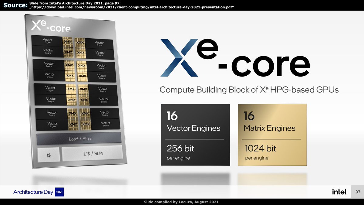
Based on Intel's architecture slide, the high-level blocks for DG2 appear to be very similar to Xe LP.
256-bit vector engines = SIMD8 Units.
Two vector engines are drawn as a pair, most likely sharing the thread control unit again .
New is a 1024-bit Matrix Engine.
5/x
256-bit vector engines = SIMD8 Units.
Two vector engines are drawn as a pair, most likely sharing the thread control unit again .
New is a 1024-bit Matrix Engine.
5/x


There will be a table with many assumptions from my side, which may turn out to be wrong.
Like I would assume that Xe HPG supports the same data inputs as Xe HPC per matrix engine.
So INT8, FP16, BF16 and TF32.
I also assume that Intel has fast FP32 accumulation at the end.
6/x
Like I would assume that Xe HPG supports the same data inputs as Xe HPC per matrix engine.
So INT8, FP16, BF16 and TF32.
I also assume that Intel has fast FP32 accumulation at the end.
6/x

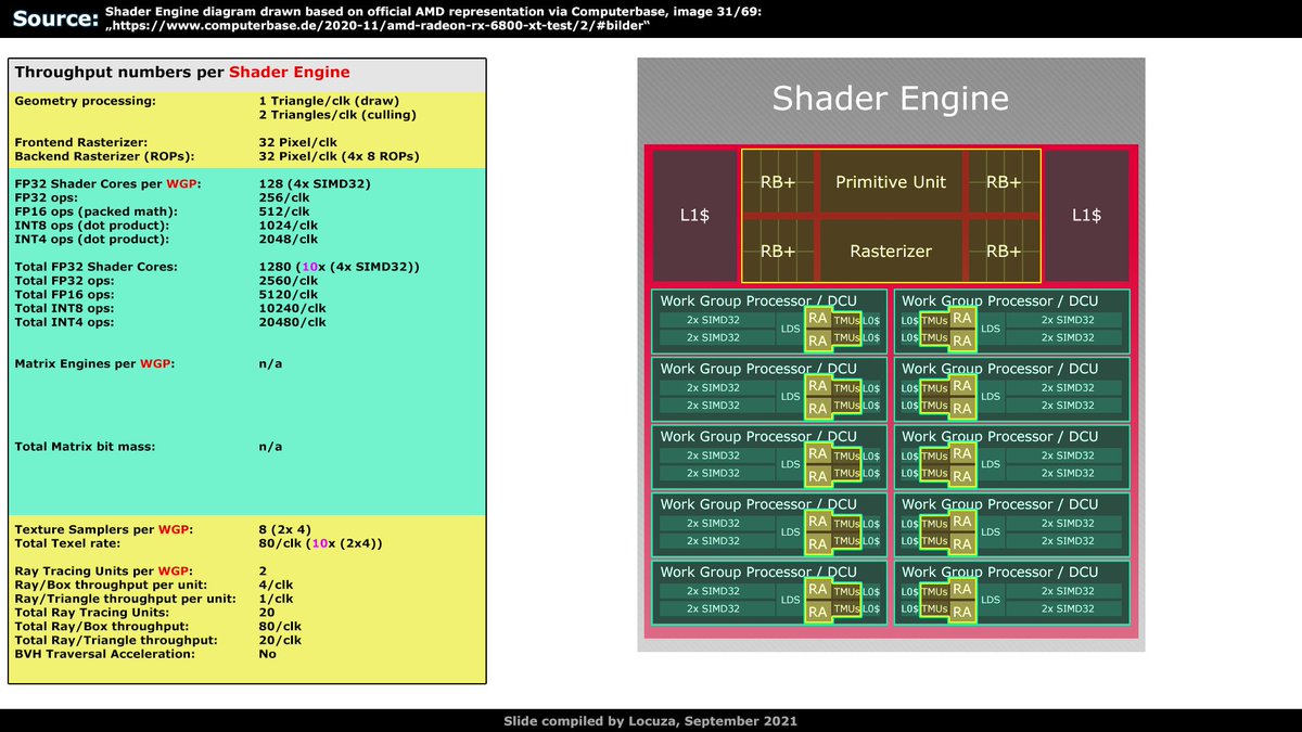
Something which Nvidia doesn't for Turing and client Ampere.
So I'm ending up with the following throughput numbers per Render Slice, Shader Engine and Graphics Processing Cluster (per clock).
I find it cool to see how the companies roughly scale their GPUs.
7/x
So I'm ending up with the following throughput numbers per Render Slice, Shader Engine and Graphics Processing Cluster (per clock).
I find it cool to see how the companies roughly scale their GPUs.
7/x


Everything inside a table.
Per high-level module Intel could have twice the FP16/BF16/TF32 throughput if they have a higher execution rate with FP32 accumulate, if not, it's the same as on Nvidia.
On paper that would be still great of course.
(Do I hear sad red noises?)
8/x
Per high-level module Intel could have twice the FP16/BF16/TF32 throughput if they have a higher execution rate with FP32 accumulate, if not, it's the same as on Nvidia.
On paper that would be still great of course.
(Do I hear sad red noises?)
8/x

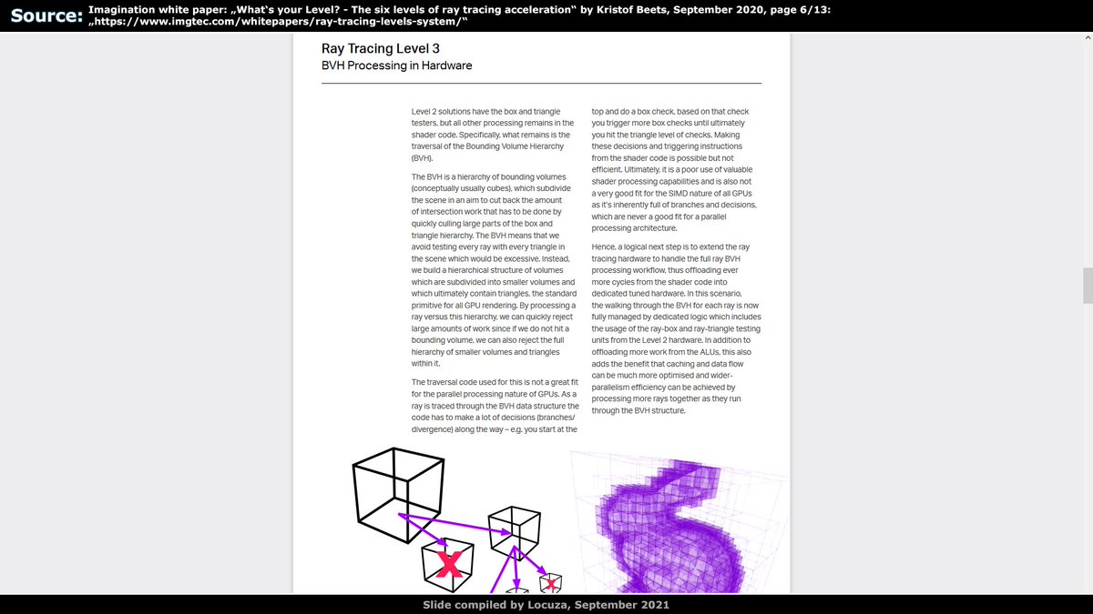
As Nvidia's RT Cores, Intel's Ray Tracing Units do support BVH traversal.
Imagination would classify it as a Level 3 Ray Tracing solution.
AMD's Ray Accelerators do not support BVH traversal, only ray/box and ray/triangle intersections are accelerated = Level 2.
9/x
Imagination would classify it as a Level 3 Ray Tracing solution.
AMD's Ray Accelerators do not support BVH traversal, only ray/box and ray/triangle intersections are accelerated = Level 2.
9/x


Currently it's not known how many ray intersections Intel's RT Units can compute, however, with BVH traversal Intel's RT performance should be quite a bit above AMD, even though the Unit count is lower.
Nvidia already shows strong performance on Turing vs. RDNA2 from AMD.
10/x
Nvidia already shows strong performance on Turing vs. RDNA2 from AMD.
10/x

Now we can look at how many high-level modules are used per chip.
DG2-512 goes ham with 8 Render Slices.
N22 uses 2 Shader Engines (but also with the highest throughput per module)
GA104 uses 6 Graphics Processing Clusters.
11/x
DG2-512 goes ham with 8 Render Slices.
N22 uses 2 Shader Engines (but also with the highest throughput per module)
GA104 uses 6 Graphics Processing Clusters.
11/x


A look at the comparison table (only per clock throughput) probably says that Navi22 does not belong there, it is a completely different class.
The 3D HW is by far the weakest, also FP32 throughput.
DG2-512 presents itself as a rasterization monster.
12/x
The 3D HW is by far the weakest, also FP32 throughput.
DG2-512 presents itself as a rasterization monster.
12/x

Obviously we have to consider the clock, which is a point where Navi22 excells.
For DG2 I took 1.8 GHz (mobile) and >2.2 GHz (desktop).
For AMD's N22 2.531 GHz (avg. clock under under 16 games at 1440p)
For GA104 1.878 & 1.920 GHz (avg. clock under 17 games at 1440p).
13/x
For DG2 I took 1.8 GHz (mobile) and >2.2 GHz (desktop).
For AMD's N22 2.531 GHz (avg. clock under under 16 games at 1440p)
For GA104 1.878 & 1.920 GHz (avg. clock under 17 games at 1440p).
13/x


Now we have the final paper comparison.
Thanks to 2.5 GHz on N22, it came much closer to the GA104 wich runs with only 1.9 GHz.
Still, many would probably say that the GA104 should lead by a strong margin.
Rasterization and FP32 throughput is much higher.
14/x
Thanks to 2.5 GHz on N22, it came much closer to the GA104 wich runs with only 1.9 GHz.
Still, many would probably say that the GA104 should lead by a strong margin.
Rasterization and FP32 throughput is much higher.
14/x

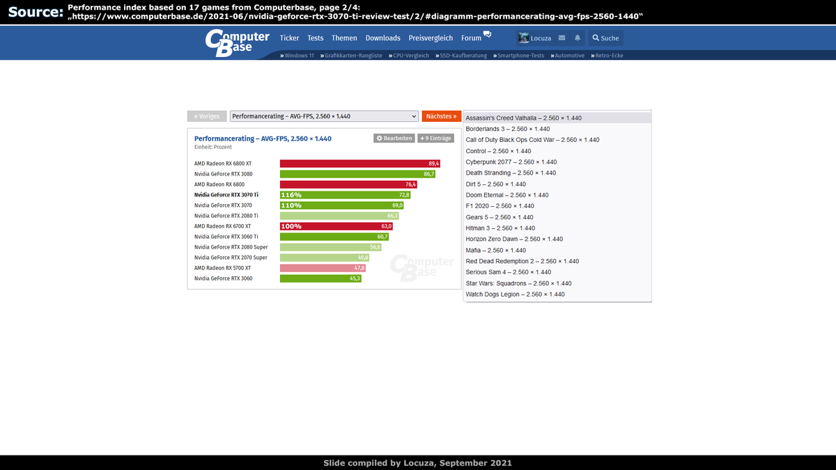
But as many know, paper specs can be far away from real performance.
The 3070 is just 10% faster than AMD's 6700 XT on a benchmark run by Computerbase.
3070 Ti wins by 16%, but it goes berserk on power consumption, memory (GDDR6X) and price (on paper :P).
We likely will..
15/x
The 3070 is just 10% faster than AMD's 6700 XT on a benchmark run by Computerbase.
3070 Ti wins by 16%, but it goes berserk on power consumption, memory (GDDR6X) and price (on paper :P).
We likely will..
15/x
..have a similar situation with DG2-512, which Intel themselves previously saw at 6700 XT/3070 level.
On paper it's a real monster.
8 Geo+Raster units with a pixel fillrate of 128 per clock.
Not even AMD's & NV's high-end chips are that wide.
4+128 on N21, 7+112 on GA102
16/x
On paper it's a real monster.
8 Geo+Raster units with a pixel fillrate of 128 per clock.
Not even AMD's & NV's high-end chips are that wide.
4+128 on N21, 7+112 on GA102
16/x


On paper DG2-512 beats GA104 in nearly all points by over 50%.
Be it triangle, pixel, texel or matrix INT8 throughput (used by XeSS/DLSS).
___
So yeah, I'm extremely looking forward to low-level benchmarks and how DG2 behaves. 😀
17/17
Be it triangle, pixel, texel or matrix INT8 throughput (used by XeSS/DLSS).
___
So yeah, I'm extremely looking forward to low-level benchmarks and how DG2 behaves. 😀
17/17

• • •
Missing some Tweet in this thread? You can try to
force a refresh


