Locuza Profile picture
Content archives: https://t.co/XOUB5IcvCc
Nov 3, 2022 22 tweets 9 min read
The N31 reveal got a couple of big surprises, in both good and bad ways.
A good surprise was AMD sharing die shots of Navi31, the GCD and MCD dies!

I took a first look at Navi31, which due to the usual pixel mess is simple and may include misinterpretations.

1/x ImageImage Awkward pause, but a few things got me thinking, and I checked a few things.
In addition, I have little time, so I have to fire those semi-random thoughts quickly.
____

Because RDNA3 has no legacy pipeline anymore, you would expect less geometry processing hardware.
The...

2/x Image
Sep 2, 2022 19 tweets 8 min read
The short Zen 4 die shot analysis is now freely available on YouTube!
Key slides and points will be also included in this Twitter thread, while the text version on Patreon and Substack will stay for paid subscribers only.

Well, actually I'm going to bed soon and may finish the Twitter thread later.
However, let's start with something.

1. Die sizes based on a package photo, a rendering of it and AMD's official product page listings.
Somebody with access should measure it directly with a caliper.
Jun 19, 2022 30 tweets 18 min read
The Alder Lake-S/P walkthrough is now freely available on Patreon, YouTube and for the first time also on Substack!
P: patreon.com/posts/die-walk…
Y:
S: locuza.substack.com/p/die-walkthro…

A few highlights and extras will be mentioned in this Twitter thread.

1/x Alder Lake-S is the first consumer chip which brought PCIe 5 support and it's always interesting to see how a new standard looks on a die shot.
With twice the transfer speed, are the PHYs larger?
AMD has PCIe3&4 blocks on basically the same node, which share the same size.

2/x
May 3, 2022 27 tweets 13 min read
This video includes what caught my eye after skimming through the open source driver patches for RDNA3.
It goes over IP versions, some feature definitions, FSR code lines & more.

Also on Patreon as a written text with images:
patreon.com/posts/65948696

1/x

This table compares the version number of the IP blocks used in AMD RDNA1, 2, and 3 discrete GPUs.

APUs and custom consoles are not taken into account.
Some IP blocks there have another major.minor.revision number.
Like Rembrandt uses SMU13.0.1 and VCN3.1.1.

2/x Image
Nov 28, 2021 34 tweets 16 min read
I proudly present... another audio mess..., I mean the second part of the DG2 Alchemist analysis and discussion.
As usual, the main points will also be covered in this twitter thread.


1/x 🧵 Die sizes of N22, GA104 and DG2-512.
Actually, the GA104 is likely closer to 400mm² with the scribe lines.
It's hard to make a fair comparison.
Different process nodes with other design trade-offs, differences in spending like for display, matrix units, ray tracing, etc.

2/x
Nov 8, 2021 25 tweets 11 min read
I finished it (!), 9 hours before AMD will officially present CDNA2/MI250X 🥳
It's basically the second rambling/analysis part for Aldebaran, going over some changes based on driver and compiler patches from AMD.
It's a technical mini spoiler, perhaps?

1/x
Disclaimer, I put that together in a short amount of time, there might be quite a few issues.
________
Because of the 110 CU notion from AMD's driver, it appears obvious to me that Aldebaran is not using 16 CUs per SE, but likely only 14 --> smaller chiplet size.

2/x
Oct 24, 2021 17 tweets 10 min read
I tried really hard to not make a multipart video series again, but it ended up to be ~1 hour long...
I had to cut it, the first part is now online, stuff I worked on since August.

Well here it is, Intel's DG2 Alchemist vs. AMD N22 and NV GA104.

1/x 🧵
The first video part is only showing theoretical throughput comparisons and how Intel, AMD and Nvidia scale their GPU configurations.
But first a bit of history, in 1998 Intel released their first dGPU, the i740, and it would be the last one till DG1 in 2021...

2/x
Aug 28, 2021 28 tweets 10 min read
And @FritzchensFritz said, "Let there be light!" and there was light:
flickr.com/photos/1305612…

Now, that the world has an incredible high quality PS5 die shot, I revisit my previous annotations and some crucial aspects are different than I thought.


1/x 🧵 It was premature from me to claim that Sony likely cut the FP pipes from 256b to 128b based on totally dark rectangles.
I should have worded it with much more uncertainty, because some people, and reportings, take it sometimes as a fact.
The custom FPU on the PS5...

2/x
Aug 27, 2021 4 tweets 3 min read
Well, @FritzchensFritz got hands on a PS5 again and did some awesome die shots!
Vanilla Zen2:
flickr.com/photos/1305612…

PS5 CPU Core:
flickr.com/photos/1305612…

The custom Zen2 CPU for Sony is only modified on the FPU side, digital logic and everything else looks identical.

1/x ImageImage 
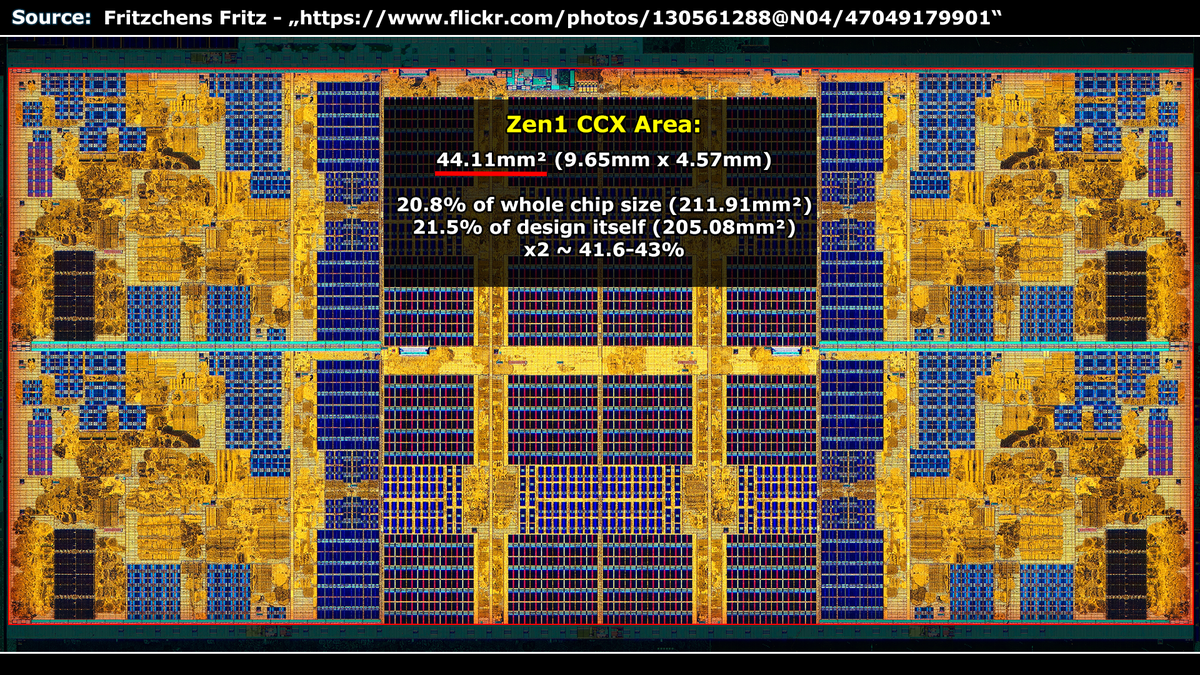
The custom FPU is now quite a bit shorter, aligning with the µcode ROM block.
Overall core size goes down from ~2.82mm² to ~2.50mm².
Vanilla Zen2 is ~13% larger, respectively the PS5 core is ~11% smaller.
Jul 19, 2021 6 tweets 2 min read
A discussion and curiosity is resolved now.
Van Gogh, which is used by Valve's Steam Deck, has 4 UMCs.
I expected 4x 16-Bit (a memory channel under LPDDR5 is actually 16-Bit wide).
The official spec claimed 5.5 Gbps (dual-channel), which didn't made sense to me.
It got corrected 
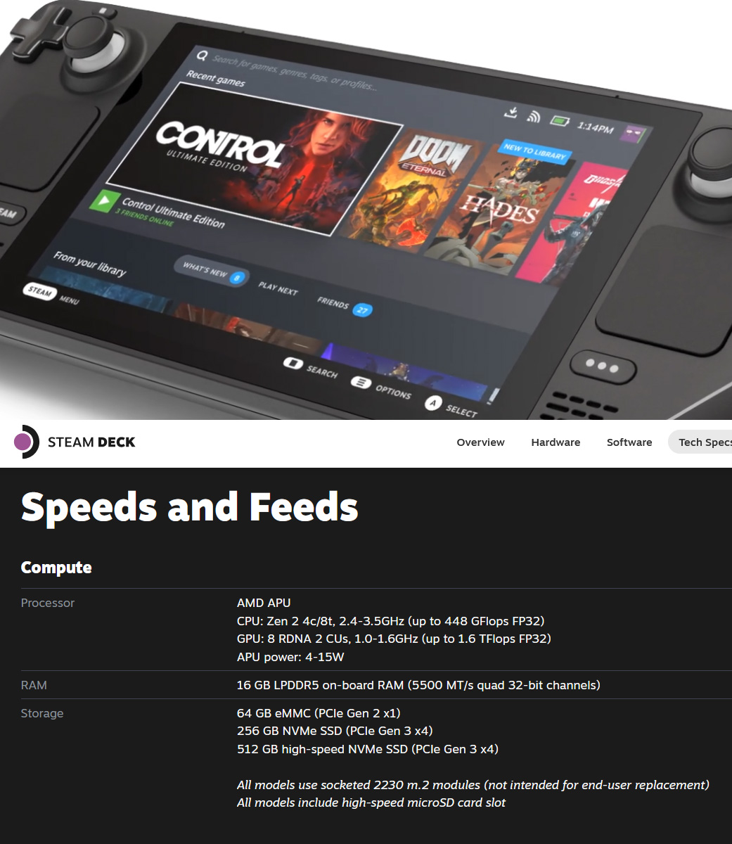
Valve claims now 4x 32-Bit (128-Bit) which fits to 4 UMCs.
It also means that as on Renoir/Cezanne, AMD is using a controller design with a 32-Bit granularity instead of 16-Bit channels.

Even 64-Bit LPDDR5 wouldn't have been bad for the Steam Deck specs but now bw looks great.
Feb 7, 2021 21 tweets 7 min read
This was a nightmare project to work on, with a frankenstein audio recording mash up but I can't muster the strength and necessary time to re-record+cut the thing again.

Topic and details are quite interesting though.
Summary pictures follow this thread.

1) Xbox Series X/S die shots scaled to relative true size.
(It's not super accurate though)
2) PS4&Xbox One die shots scaled to relative true size
3.) ^ with annotations

If people are curious about the PS4/Xbox One gen, I could make an extra video for them. ImageImageImage
Sep 2, 2020 30 tweets 8 min read
Ahh damn it, I again didn't managed a super fast rambling video about Renoir vs. Tiger Lake.
So it's time for a picture thread with rambling, less than 30 minutes to go.
1/x 
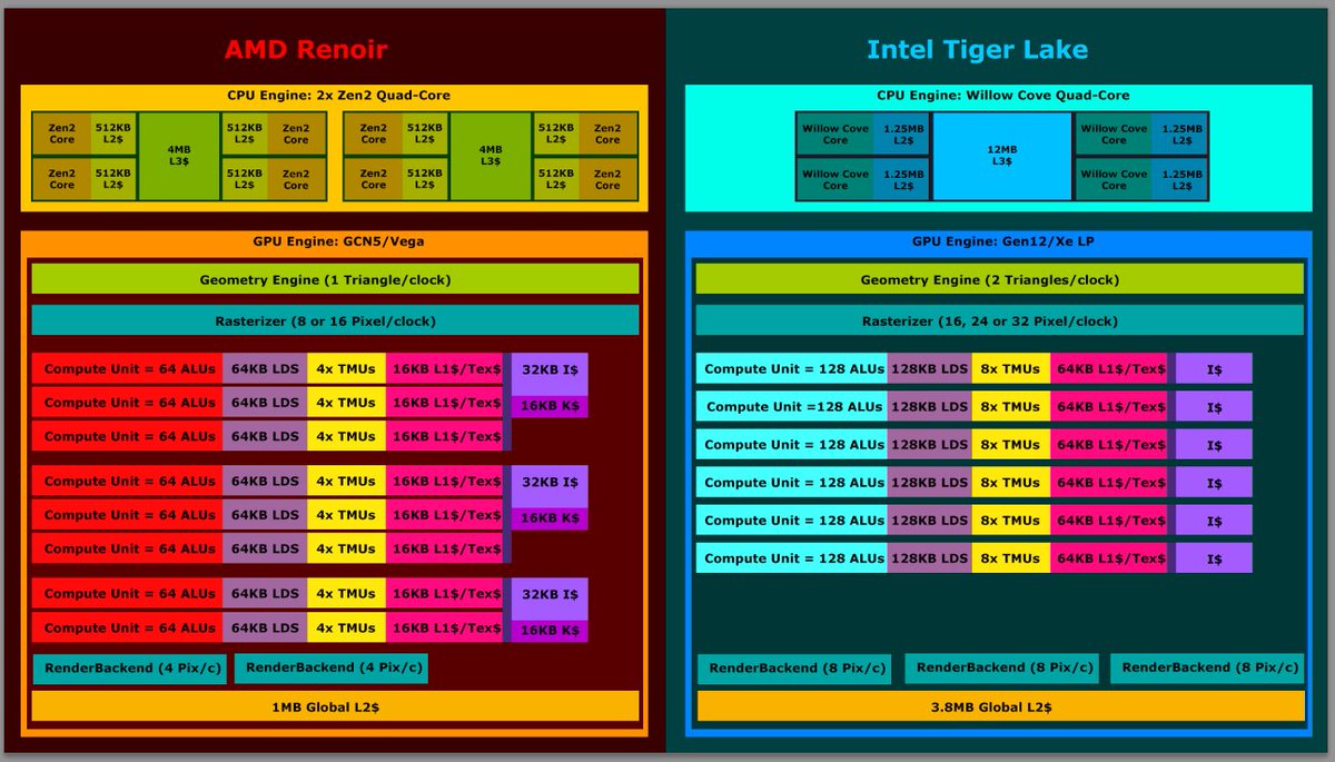
I really like the CPU engine from Intel.
Willow Cove has a massive amount of cache and should do over 20% better per clock than Renoir.
Under 15-30W I'm also sceptical how well the 8 cores on Renoir scale but the results are out there, I just didn't had the time to look.
2/x
Sep 1, 2020 20 tweets 5 min read
I think even for a speed rambling video the time is too short with Ampere's presentation coming in less than three hours which is why a picture thread with my thoughs will follow.
Ampere vs. Big Navi.🔥
1/x The specs with 5248 "CUDA cores" are already out there for the GTX3090.
@_rogame found the configuration of Navi21 from driver files, confirming that 40WGPs/80CUs/5120 "cores" will be used.
Bringing both close together in terms of FP32 throughput
2/x
Jul 24, 2020 7 tweets 5 min read
Zen 2 (+1) part 6 analysis for laymen is done:


Comparing the sizes of CCX, L3$, L2$, Core and starting with the L3$ item/device inventory.
Images with crucial information follow this tweet. 1) Technical details and differences between Zen1 and Zen2
2) Zen1 CCX size of 44.11mm²
3) Zen2 CCX size of 31.39mm²