
I finished it (!), 9 hours before AMD will officially present CDNA2/MI250X 🥳
It's basically the second rambling/analysis part for Aldebaran, going over some changes based on driver and compiler patches from AMD.
It's a technical mini spoiler, perhaps?
1/x
It's basically the second rambling/analysis part for Aldebaran, going over some changes based on driver and compiler patches from AMD.
It's a technical mini spoiler, perhaps?
1/x
Disclaimer, I put that together in a short amount of time, there might be quite a few issues.
________
Because of the 110 CU notion from AMD's driver, it appears obvious to me that Aldebaran is not using 16 CUs per SE, but likely only 14 --> smaller chiplet size.
2/x
________
Because of the 110 CU notion from AMD's driver, it appears obvious to me that Aldebaran is not using 16 CUs per SE, but likely only 14 --> smaller chiplet size.
2/x


According to the patches, on Aldebaran always 2 CUs share 1x 32KiB I$ and 1x 16KiB K$.
1st image shows how the shader array is build on Vega10, Arcturus (CDNA1) and Aldebaran (CDNA2)
____
Aldebaran has a prefetch depth of 16 cache lines.
It's only 3 on RDNA/GFX10.
3/x
1st image shows how the shader array is build on Vega10, Arcturus (CDNA1) and Aldebaran (CDNA2)
____
Aldebaran has a prefetch depth of 16 cache lines.
It's only 3 on RDNA/GFX10.
3/x


It's a bit funny that only Aldebaran and GFX10 are mentioned, instruction prefetch was a bullet-point for GCN4/Polaris.
Besides I$/K$, L1D$ is still just 16KB small, 8MB for the L2$ and LDS also should be just 64KB.
That's not so great, if it really ends up this way.
4/x
Besides I$/K$, L1D$ is still just 16KB small, 8MB for the L2$ and LDS also should be just 64KB.
That's not so great, if it really ends up this way.
4/x

What is great, is the redesigned register file.
Instead of 64KB VGPRs + 64KB AGPRs (not useable by vector SIMD), CDNA2 will have a unified 128KB reg file.
The split is programmable and the vector SIMD should be able to access it fully if no matrix ops are used.
5/x
Instead of 64KB VGPRs + 64KB AGPRs (not useable by vector SIMD), CDNA2 will have a unified 128KB reg file.
The split is programmable and the vector SIMD should be able to access it fully if no matrix ops are used.
5/x

AMD changed the VGPR allocation granularity from 4 to 8, they did the same from RDNA1 to RDNA2.
I guess that's a better trade-off and over-allocation does not happen often.
6/x
I guess that's a better trade-off and over-allocation does not happen often.
6/x

The vector SIMDs got a huge upgrade.
SP/DP implementation is a fascinating topic with unfortunately not so accessible information.
My interpretation, AMD is using mixed-precision ALUs for FP32 and FP64 ops.
Nvidia uses separate FP64 units, trading area for better efficiency.
7/x
SP/DP implementation is a fascinating topic with unfortunately not so accessible information.
My interpretation, AMD is using mixed-precision ALUs for FP32 and FP64 ops.
Nvidia uses separate FP64 units, trading area for better efficiency.
7/x

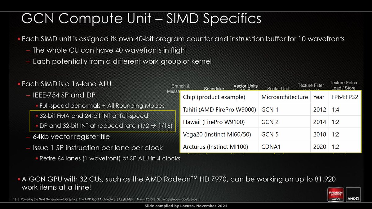

IIRC VLIW5 was the first hw for AMD with FP64 support, FP64:FP32 ratio was 1:5 (not on all GPUs).
On GCN it's configurable from 1:2 (Half-Rate) to 1:16.
That's the limit since 2014 with Hawaii (FirePro).
Why no 1:1/Full Rate option?
I remember...
8/x
On GCN it's configurable from 1:2 (Half-Rate) to 1:16.
That's the limit since 2014 with Hawaii (FirePro).
Why no 1:1/Full Rate option?
I remember...
8/x
...some old forum discussions on @3DCenter_org, arguing that full-rate is not such a great idea for any market which also needs FP32, because with a bit of extra logic, FP64 hw can process FP32 faster, so FP64 full-rate would be rather FP32 slow-rate.
9/x
9/x
It's a subject beyond my layman's knowledge.
I would love more information in that regard and how it really looks like.
Anyway, CDNA2 comes with full-rate FP64 support. ;)
Also 64 Data Parallel Primitives for cross lane operations.
10/x
I would love more information in that regard and how it really looks like.
Anyway, CDNA2 comes with full-rate FP64 support. ;)
Also 64 Data Parallel Primitives for cross lane operations.
10/x

My simplified view on this is that the internal bit-width of the ADD/MUL logic was increased.
I simply describe it as 64-Bit lanes vs. 32-Bit lanes previously.
It may not be really accurate but I think it checks out on how it effectively works.
11/x
I simply describe it as 64-Bit lanes vs. 32-Bit lanes previously.
It may not be really accurate but I think it checks out on how it effectively works.
11/x

AMD is going to keep 4-cycle issue and not building a different execution model.
So I think the SIMD units still have 16 lanes and you can either process 1x FP64 or 1xFP32 or 1x FP16 op.
Same throughput for all, unless you use packed math instructions...
12/x
So I think the SIMD units still have 16 lanes and you can either process 1x FP64 or 1xFP32 or 1x FP16 op.
Same throughput for all, unless you use packed math instructions...
12/x
GCN3/4 only had same rate FP16 ops, GCN5 brought packed-math for FP16.
2x FP16 inputs are loaded and the same operation applied to both, doubling the throughput while being still executed by only one SIMD lane.
CDNA2 uses the same trick for FP32, new are packed FP32 instr.
13/x
2x FP16 inputs are loaded and the same operation applied to both, doubling the throughput while being still executed by only one SIMD lane.
CDNA2 uses the same trick for FP32, new are packed FP32 instr.
13/x

Driver patches don't mention something like quad-packed FP16, so packed FP32 and packed FP16 ops have now the same theoretical throughput.
In comparison to CDNA1 you get twice the FP64 throughput and FP32 throughput.
Unified reg files comes in handy to feed this.
14/x
In comparison to CDNA1 you get twice the FP64 throughput and FP32 throughput.
Unified reg files comes in handy to feed this.
14/x
Now the Matrix v2 units did not get a huge upgrade.
It's my understanding that the BF16 rate was doubled, making it equal to FP16 throughput, which was not the case on CDNA1.
A new capability is matrix FP64 support.
Half-rate vs. FP32.
Otherwise apparently no upgrades.
15/x
It's my understanding that the BF16 rate was doubled, making it equal to FP16 throughput, which was not the case on CDNA1.
A new capability is matrix FP64 support.
Half-rate vs. FP32.
Otherwise apparently no upgrades.
15/x


No TF32 support or even higher BF16, FP16 or INT8 throughput.
In fact you should get now the same FP32 and FP64 throughput on vector or matrix units.
It's clear that AMD's focus was on the vector side, with rather little matrix innovations.
16/x
In fact you should get now the same FP32 and FP64 throughput on vector or matrix units.
It's clear that AMD's focus was on the vector side, with rather little matrix innovations.
16/x
Now the money slides...
Nvidia A100 vs. AMD MI100 & MI250X vs. Intel Ponte Vecchio.
Let's start with the good things on paper.
FP64 throughput is very high, competitive with PVC unless Intel significantly increases clocks.
A0 PVC silicon runs with ~1.4 GHz.
Nvidia A100 vs. AMD MI100 & MI250X vs. Intel Ponte Vecchio.
Let's start with the good things on paper.
FP64 throughput is very high, competitive with PVC unless Intel significantly increases clocks.
A0 PVC silicon runs with ~1.4 GHz.


With FP32 the MI250X is the king of the hill.
Intel has full-rate FP64 but no packed-math for FP32, AMD wins basically by factor 2.
AMD is also the only one who supports matrix FP32 ops.
_
Now the bad things, AMD is clearly not focused on low-precision throughput.
18/x
Intel has full-rate FP64 but no packed-math for FP32, AMD wins basically by factor 2.
AMD is also the only one who supports matrix FP32 ops.
_
Now the bad things, AMD is clearly not focused on low-precision throughput.
18/x

Intel wins that paper battle by factor 2 (FP/BF16).
MI250X is beating the A100, but it's using more silicon and has a higher power rating, not to mention that A100 is on the market since a long time.
For matrix INT8 applications MI250X gets beaten badly.
19/x
MI250X is beating the A100, but it's using more silicon and has a higher power rating, not to mention that A100 is on the market since a long time.
For matrix INT8 applications MI250X gets beaten badly.
19/x


What looks in general terrible on Aldebaran is the memory subsystem.
Per CU AMD is still using a tiny 16KB L1D$ and 64KB for scratchpad memory, combined 80KB worth of storage.
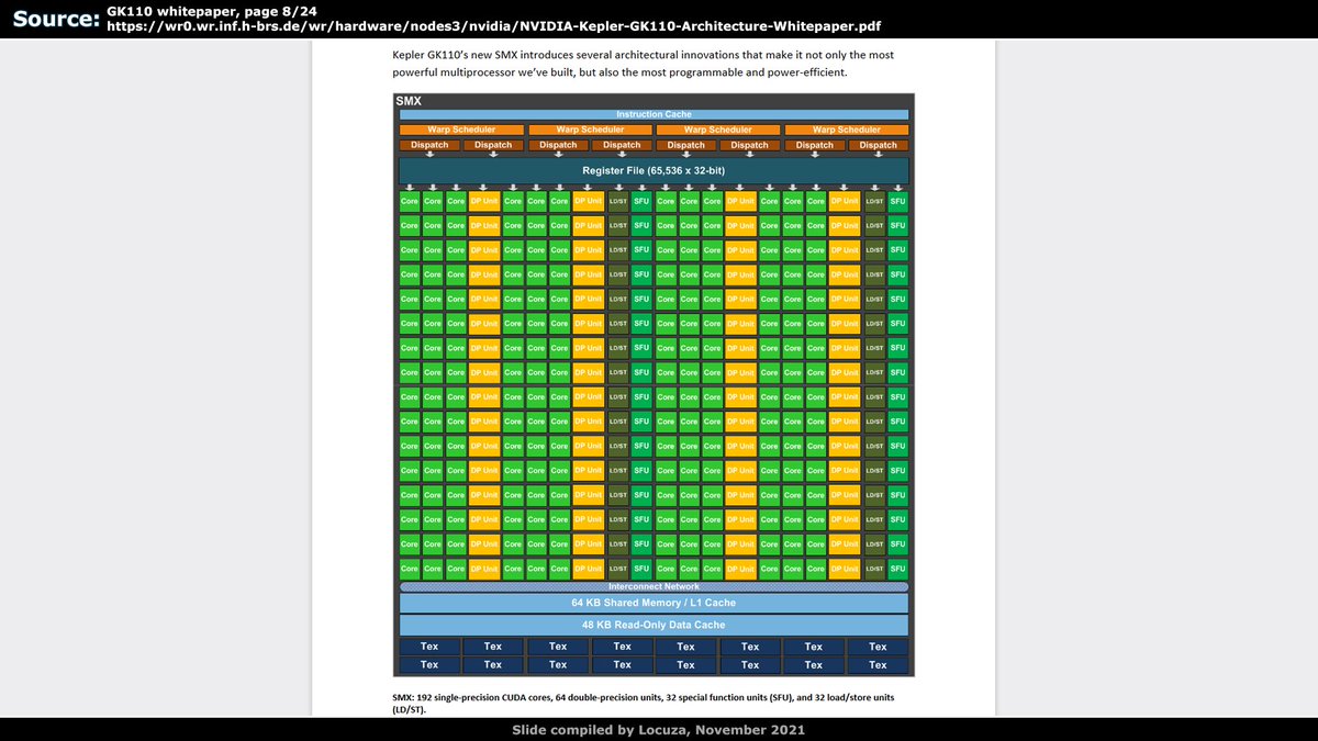
A100 uses 192KB per SM, it's configurable and can support larger L1$ or scratchpad sizes.
20/x
Per CU AMD is still using a tiny 16KB L1D$ and 64KB for scratchpad memory, combined 80KB worth of storage.
A100 uses 192KB per SM, it's configurable and can support larger L1$ or scratchpad sizes.
20/x


Intel goes bonkers with 512KB per Xe Core.
In total you have ~17.19MB on MI250X, 20.25MB on A100 and 64MB on PVC.
And then there is the L2$.
A100 has 40MB L2$ (48 physically), Aldebaran according to driver patches just 8MB per chiplet, 16MB in total.
Intel -> 2x144MB L2$..
21/x
In total you have ~17.19MB on MI250X, 20.25MB on A100 and 64MB on PVC.
And then there is the L2$.
A100 has 40MB L2$ (48 physically), Aldebaran according to driver patches just 8MB per chiplet, 16MB in total.
Intel -> 2x144MB L2$..
21/x


I think AMD will heavily rearchitect the cache hierarchy on RDNA3 and CDNA3.
L1$ & LDS have to be unified or enlarged, the LLC is great on RDNA2 and will get better on RDNA3, but
CDNA3 has to get it too.
I'm not sure if CDNA2 has surprises in store for today (cache) ?
22/x
L1$ & LDS have to be unified or enlarged, the LLC is great on RDNA2 and will get better on RDNA3, but
CDNA3 has to get it too.
I'm not sure if CDNA2 has surprises in store for today (cache) ?
22/x
To some extent this paperwork doesn't really matter. Real product performance and business deals do.
AMD got "at least" the first western exascale deal with Frontier, great achievement.
One big reason was the coherent link between CDNA2 and Trento (custom Milan).
23/x
AMD got "at least" the first western exascale deal with Frontier, great achievement.
One big reason was the coherent link between CDNA2 and Trento (custom Milan).
23/x

Device memory is cachable by Trento.
However, I wonder if it's already using the 3rd Gen Infinity Architecture or some pre-form of it?
There are many other questions, like who gets access to Trento?
Who has to wait for Genoa for a coherent link between CDNA2+ and CPUs?
24/x
However, I wonder if it's already using the 3rd Gen Infinity Architecture or some pre-form of it?
There are many other questions, like who gets access to Trento?
Who has to wait for Genoa for a coherent link between CDNA2+ and CPUs?
24/x

In 7 hours we hopefully will get some answers.
Before I forgot to mention it, CDNA2 supports a threadgroup split mode, bypassing L1$/LDS memory to schedule waves from a workgroup on any compute unit.
I don't know what the specific application field of that would be.
25/25
Before I forgot to mention it, CDNA2 supports a threadgroup split mode, bypassing L1$/LDS memory to schedule waves from a workgroup on any compute unit.
I don't know what the specific application field of that would be.
25/25
• • •
Missing some Tweet in this thread? You can try to
force a refresh


