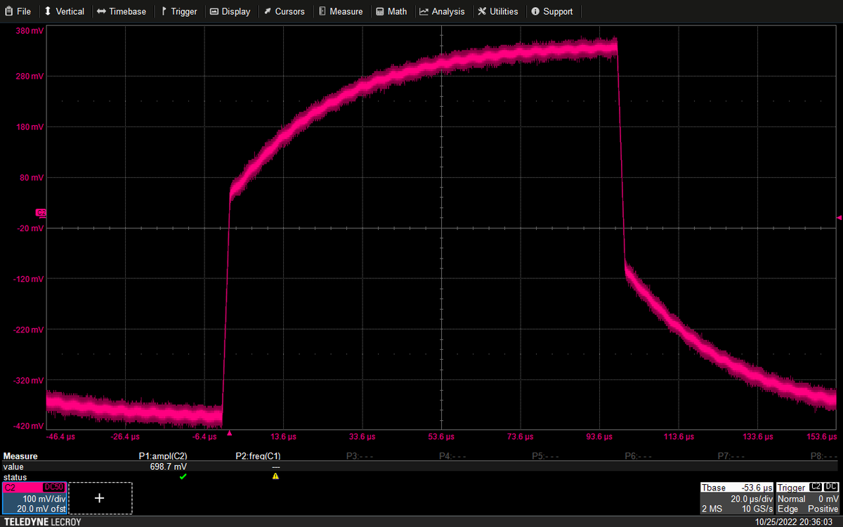
A week or so ago, @femtoduino asked me to help out with troubleshooting and reworking a prototype of the BOMU, a tiny USB-connected microcontroller dev board. It's a super dense six-layer board with multiple levels of blind vias.
Here's a bare board after removal of back mask.
Here's a bare board after removal of back mask.


So far, there's two known problems with it.
1) A blind via from layer 2 to 6 collides with a trace on layer 3. This is a design bug that slipped through DRC somehow, and results in SWCLK being shorted to a power rail.
1) A blind via from layer 2 to 6 collides with a trace on layer 3. This is a design bug that slipped through DRC somehow, and results in SWCLK being shorted to a power rail.


Correction, from layer 3 to 6 collides with a trace on 4.
The good news is that there's no polygons on layer 2 in this area at all. While the USB connector footprint does cover it on layer 1, repairing a solid copper plane after an inner layer edit is straightforward.
The good news is that there's no polygons on layer 2 in this area at all. While the USB connector footprint does cover it on layer 1, repairing a solid copper plane after an inner layer edit is straightforward.
I plan to approach the region of interest from the layer 1 side (even though it's further away) because there's relatively few obstacles to navigate. By comparison, coming from layer 6 would involve doing an inner layer edit under a WLCSP.
Even I don't want to do *that*.
Even I don't want to do *that*.
But there's also a second short: the net on the circled pad is shorted to ground *somewhere*. We haven't been able to locate an obvious design error in the gerbers, suggesting a manufacturing defect.
And I can't rework a short I can't find.
And I can't rework a short I can't find.
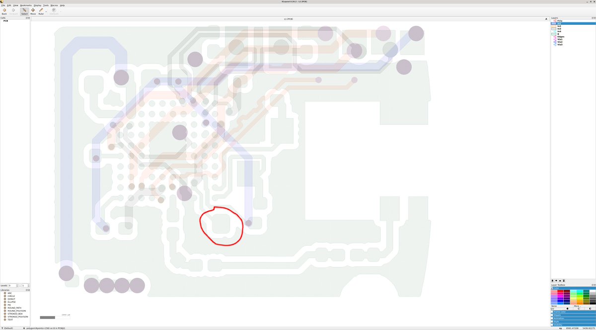
The good news is that it appears the entire prototype lot is affected, so it's probably one marginal bit of clearance that is bridging due to underetch. If we can find the short on one board, all the others are probably shorting in the same spot.
Unfortunately I don't have an X-ray system, but we do have multiple boards.
So I'm going to try old school mechanical tomography - sanding down the board a layer at a time and photographing the exposed surfaces as I go.
It's a straightforward, though destructive, process.
So I'm going to try old school mechanical tomography - sanding down the board a layer at a time and photographing the exposed surfaces as I go.
It's a straightforward, though destructive, process.
I cast one of the unpopulated boards into a puck of clear epoxy.
The embedding process is exactly the same as for my cross section samples (), except the board is parallel rather than perpendicular to the plane of polishing, and I'm using coarser abrasives
The embedding process is exactly the same as for my cross section samples (), except the board is parallel rather than perpendicular to the plane of polishing, and I'm using coarser abrasives


Nothing more I can do until the epoxy cures, and that will be pretty late Thursday evening so I probably won't be able to start the sanding process until Friday after work.
Stay tuned for updates then!
Stay tuned for updates then!
Update: I think I found the second short. I'm still going to do the tomography process since the board is already in epoxy and useless for anything else, so I might as well make sure there's no OTHER bugs.
This blind via goes from L4-L6, but the pad grazes a ground plane on L5.
This blind via goes from L4-L6, but the pad grazes a ground plane on L5.

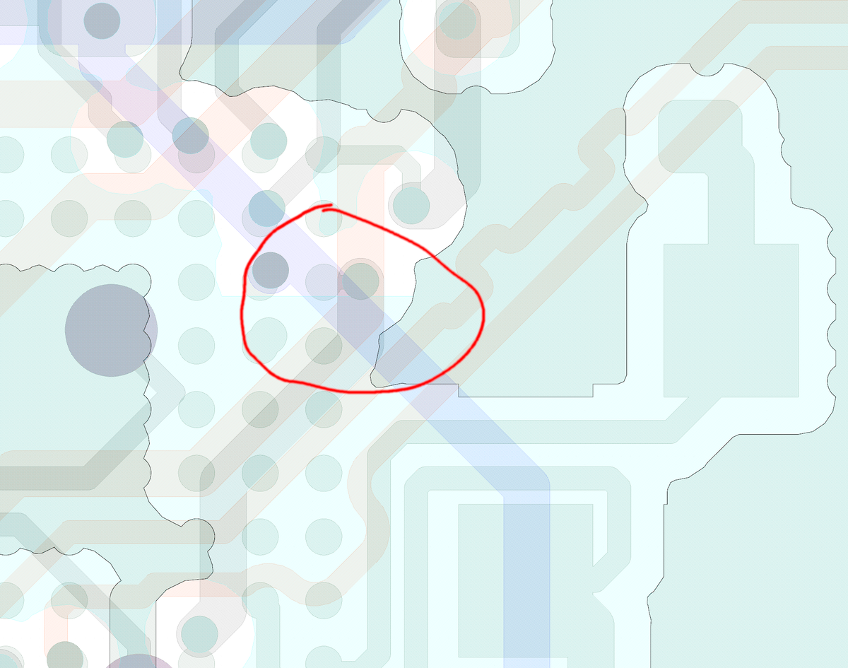
Good news: We know where it is.
Bad news: getting to it is not going to be fun. I can come from the back side (which would require removing the WLCSP, milling down to layer 5, then cutting the via pad away from the ground plane).
Bad news: getting to it is not going to be fun. I can come from the back side (which would require removing the WLCSP, milling down to layer 5, then cutting the via pad away from the ground plane).
Coming from the front avoids the WLCSP rework.
But I'd have to cut through the USB connector pad on L1, a power trace on L2, a signal trace on L3, and a signal trace on L4 before I get to the short.
Then patch it all up on my way out.
But I'd have to cut through the USB connector pad on L1, a power trace on L2, a signal trace on L3, and a signal trace on L4 before I get to the short.
Then patch it all up on my way out.
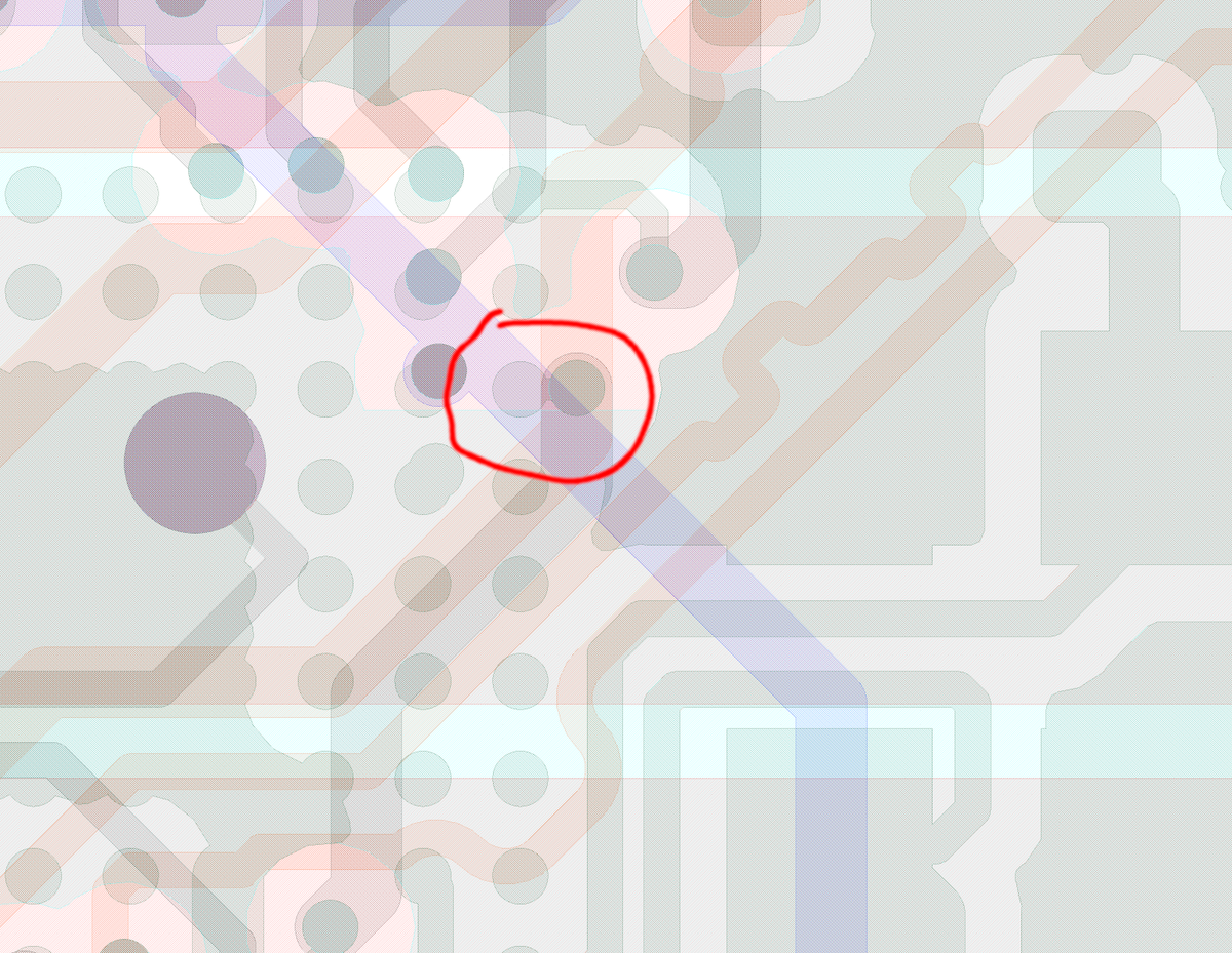
And do all of that at the bottom of a high aspect ratio hole.
No matter which route I go, this is going to be an epic bodge job. It's probably going to dethrone the time I drilled out the vias to a QFN thermal slug and reconnected them to a different net on L7 of an 8L board.
No matter which route I go, this is going to be an epic bodge job. It's probably going to dethrone the time I drilled out the vias to a QFN thermal slug and reconnected them to a different net on L7 of an 8L board.
Ok so, it's Friday. I was planning on starting the tomography but the epoxy isn't quite cured yet, so I'm going to try the actual rework on one of the bare boards.
The first short should be fairly easy to clear. It's a L3-L6 blind via, shorted to a signal trace on L4.
There's nothing in the way above the region of interest except for the USB D- pin which should be easy to touch up after.
There's nothing in the way above the region of interest except for the USB D- pin which should be easy to touch up after.

One potential wrinkle is the fact that I need to get down to L4 to clear the short, but I still need the via to be intact.
I think the easiest option is going to be to start with a fairly large cavity (say 500 μm x 500 μm) going through L1/L2 and exposing L3 in the region of interest.
This will be around a 325 μm deep milling operation.
This will be around a 325 μm deep milling operation.
The problem is, I then need to go down another ~1050 μm to reach L4, where the short is. And that might be hard at the bottom of a deep hole, but we'll see how things look. The west side of the ROI is completely empty, so if I need to elongate the mill cavity I can do that.
In either case, once I reach L4 the actual circuit edit is relatively straightforward.
Off to the mill, wish me luck...
Off to the mill, wish me luck...
Initial setup on the mill.


Indexing off the top left corner of the USB D- pad so I can get close to the target location
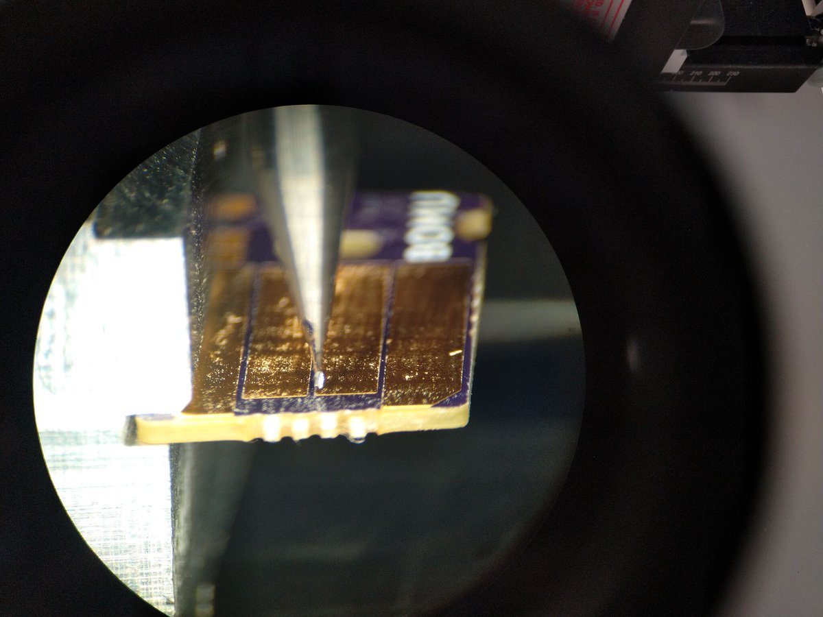
Ready to start cutting
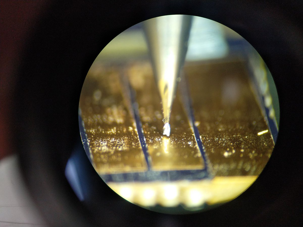
Initial exploratory cut. This was freehanded with no backlash compensation, but the outline of the cavity at this stage isn't too crucial.
The main cavity is about 480 x 600 μm. I'll make it larger in the horizontal axis, the angled microscope means it's hard to see the floor.
The main cavity is about 480 x 600 μm. I'll make it larger in the horizontal axis, the angled microscope means it's hard to see the floor.
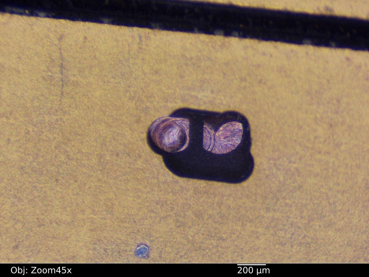
Center of the cavity is 2010 μm right and 730 μm down from the top left corner. Right where I was aiming for.
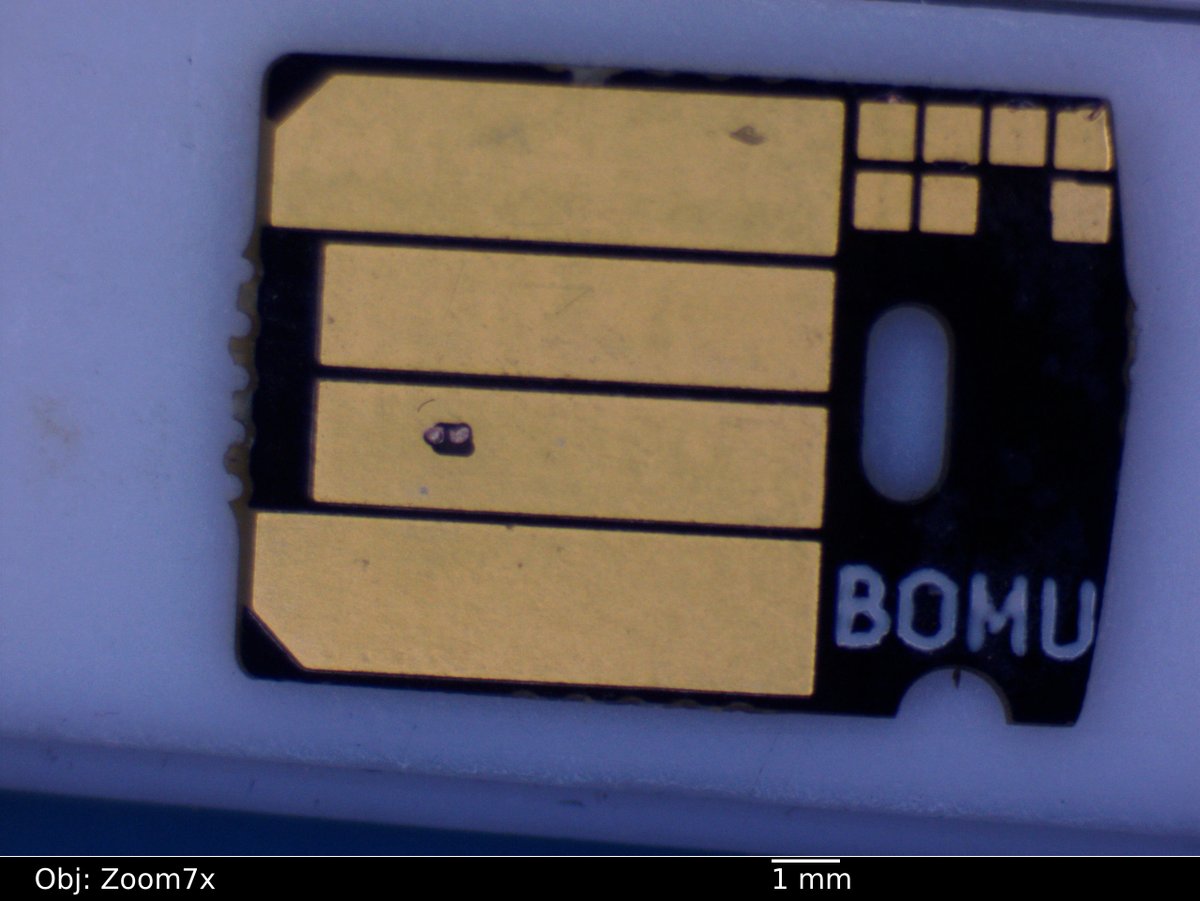
Overlaying the gerbers on the optical image, we can see the cut position is dead on. The copper visible at the bottom of the mill cavity is the via pads (which are slightly larger than spec).

The next step is going to be to extend the cavity to the south and west, so I have a bit of room to work without endangering the traces on layer 3.
I want a fairly large hole here since I need to be able to see the floor of the cavity (on the east side at least) for the edit.
I want a fairly large hole here since I need to be able to see the floor of the cavity (on the east side at least) for the edit.
Aaand that's not good!
I made a cut that should have been quite conservative based on the stackup, and ended up cutting through layers 4 and 5.
Upon further investigation, it seems that @femtoduino linked me to a 1.6mm thick stackup but this board is only 0.8 mm thick.
I made a cut that should have been quite conservative based on the stackup, and ended up cutting through layers 4 and 5.
Upon further investigation, it seems that @femtoduino linked me to a 1.6mm thick stackup but this board is only 0.8 mm thick.

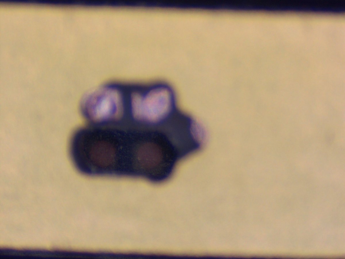
So a milling operation that should have taken me from layer 3 down about halfway to layer 4 ended up going through 4 and 5 and almost hitting 6.
I should have caught this when the board didn't fit my jig designed for 1.6mm thick PCBs. Derp.
I should have caught this when the board didn't fit my jig designed for 1.6mm thick PCBs. Derp.
The good news is, it looks like the only thing I damaged was a bit of ground plane and the trace I was going to cut anyway.
So I might still have a shot at salvaging this board. I just need to expose layer 4 at either side of this trace and reconnect the broken halves.
So I might still have a shot at salvaging this board. I just need to expose layer 4 at either side of this trace and reconnect the broken halves.
I also have one other blank board to practice on before I try reworking one of the three populated boards. And I learned a valuable lesson.
Before I continue on this board, it looks like the tomography sample is cured so time to sand it a bit.
Before I continue on this board, it looks like the tomography sample is cured so time to sand it a bit.
Here's layer 6, via 5-6, and layer 5.
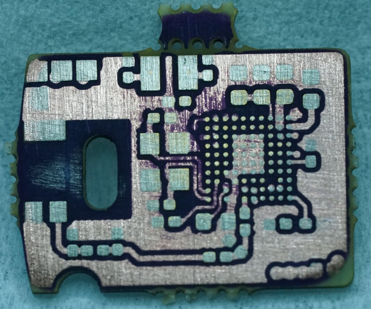
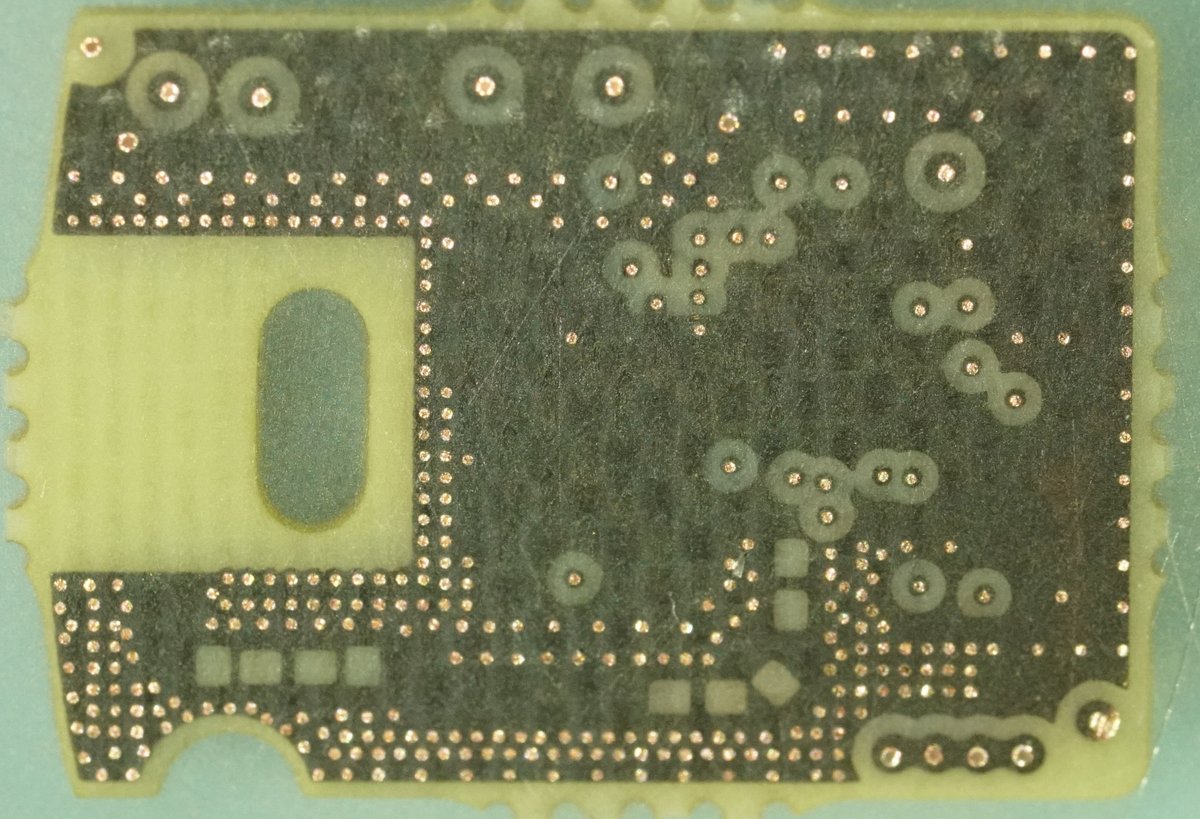
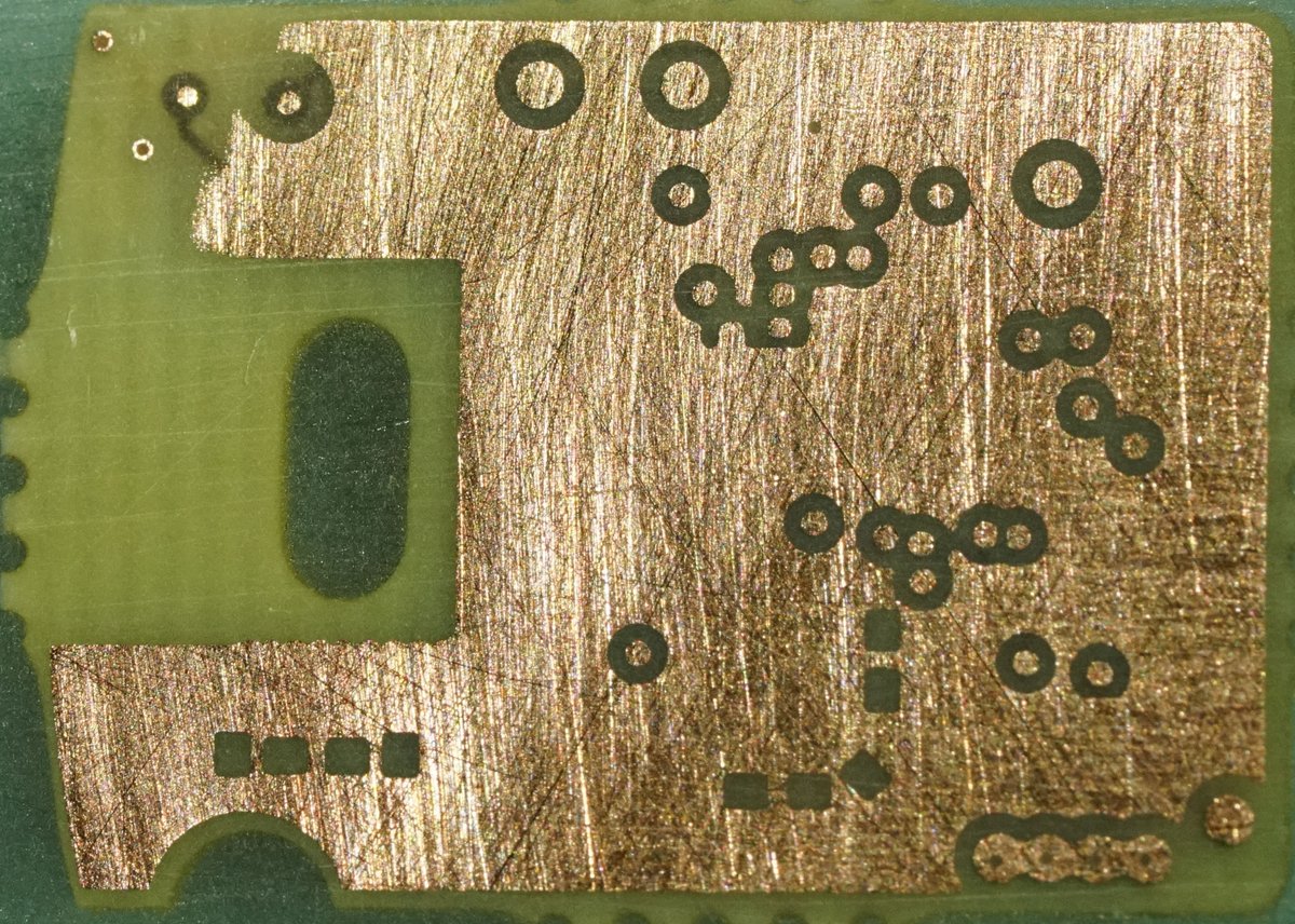
And that's a short if I ever saw one...
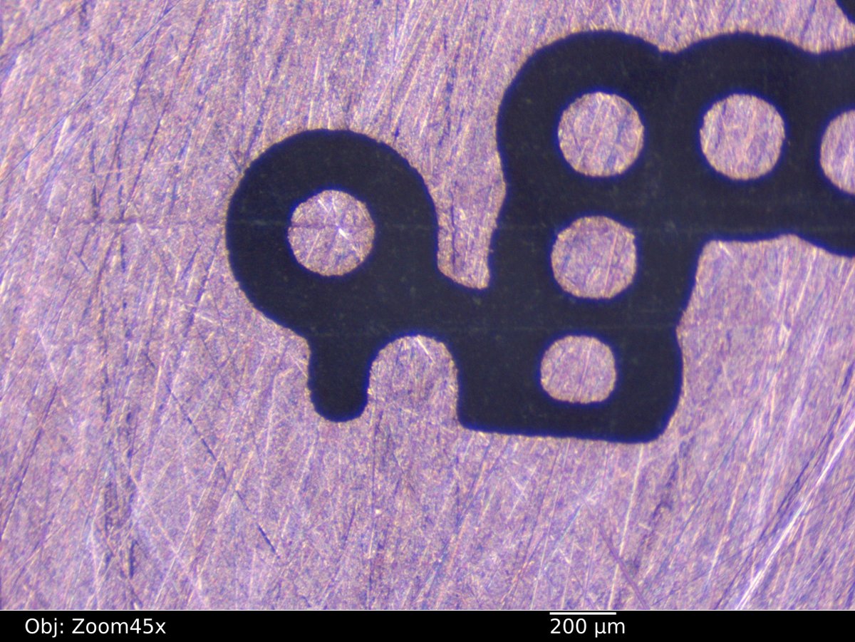
Time for a bit more polishing: Via 4-5 and metal 4.
And our second short.
And our second short.

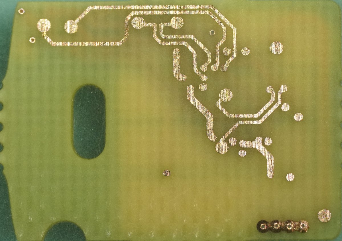

Via 3-4 and metal 3. I had to go through the board core - a fairly large distance with no planarity references. Ended up slightly off level, as you can see in the bottom right.
But I think we can still see everything we need.
But I think we can still see everything we need.
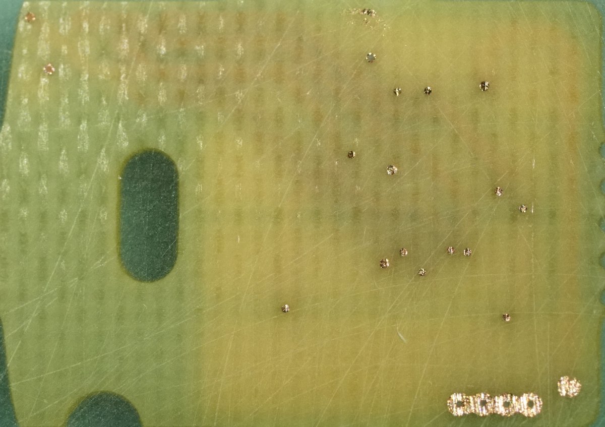

Via 1-2 and metal 2.
Seems like I forgot to grab a pic of via 2-3 :(
Seems like I forgot to grab a pic of via 2-3 :(


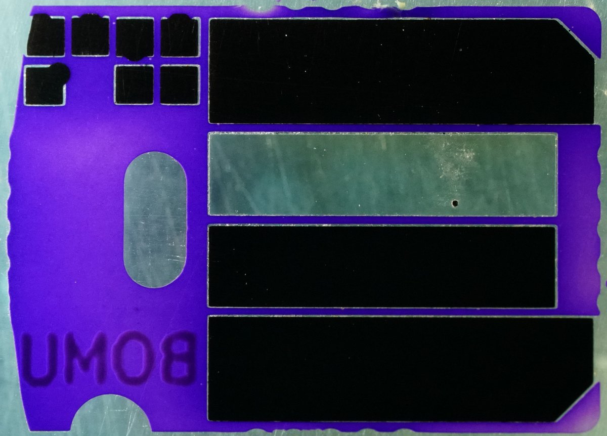
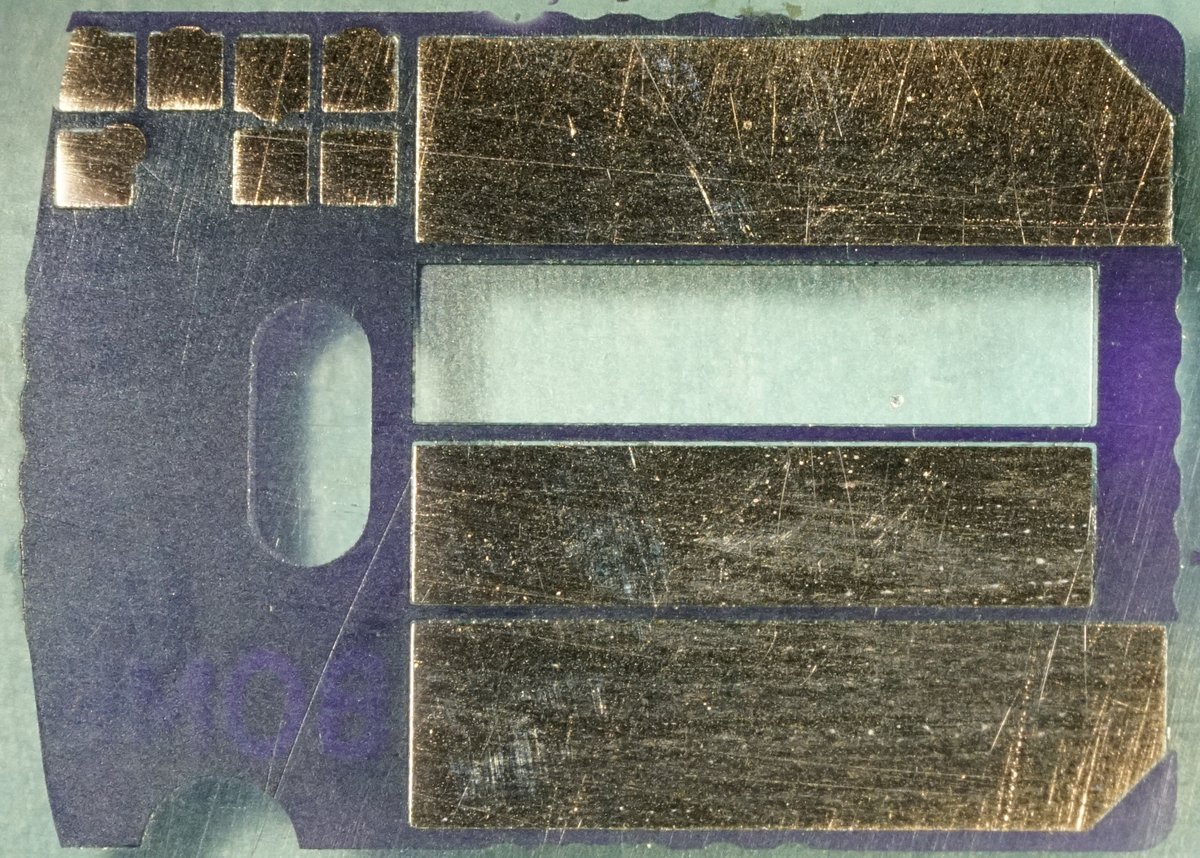
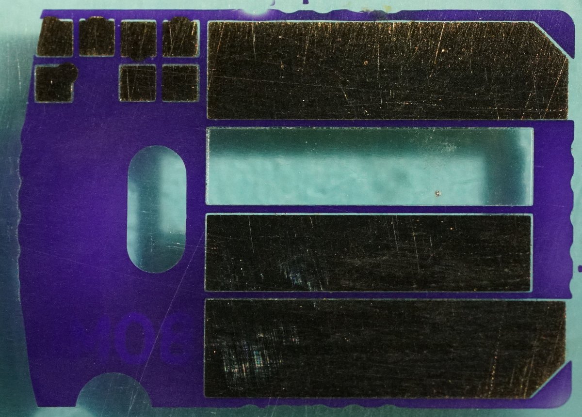
And finally, metal 1. Not strictly necessary but why not?
I decided to put a bit of extra effort into getting a really nice surface finish here. One of the USB pins delaminated, sadly, but I think it still looks really nice especially when backlit.
I decided to put a bit of extra effort into getting a really nice surface finish here. One of the USB pins delaminated, sadly, but I think it still looks really nice especially when backlit.
Back to the lab. Going to try and successfully rework the first short (the L-shaped trace on layer 4 shorting to the via).
To recap, I was given incorrect stackup info and cut a little too deep, damaging the trace. So now I have to fix it.
To recap, I was given incorrect stackup info and cut a little too deep, damaging the trace. So now I have to fix it.
Here's the current setup for another cut. To recap. we're trying to fix a short where a blind via shorts to a signal trace. I've rotated the layer view so it lines up with the microscope view.
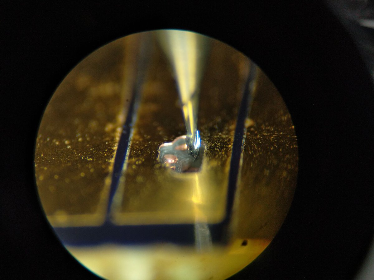
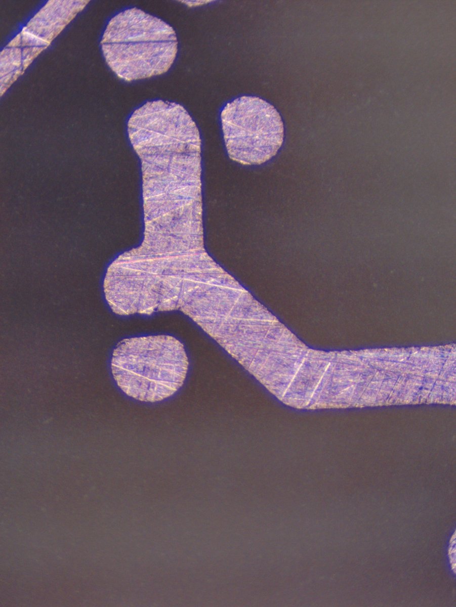
These images are at 45x, as far as my stereo microscopes can go. We've exposed the trace and can solder to it, but it looks like the short isn't broken yet.
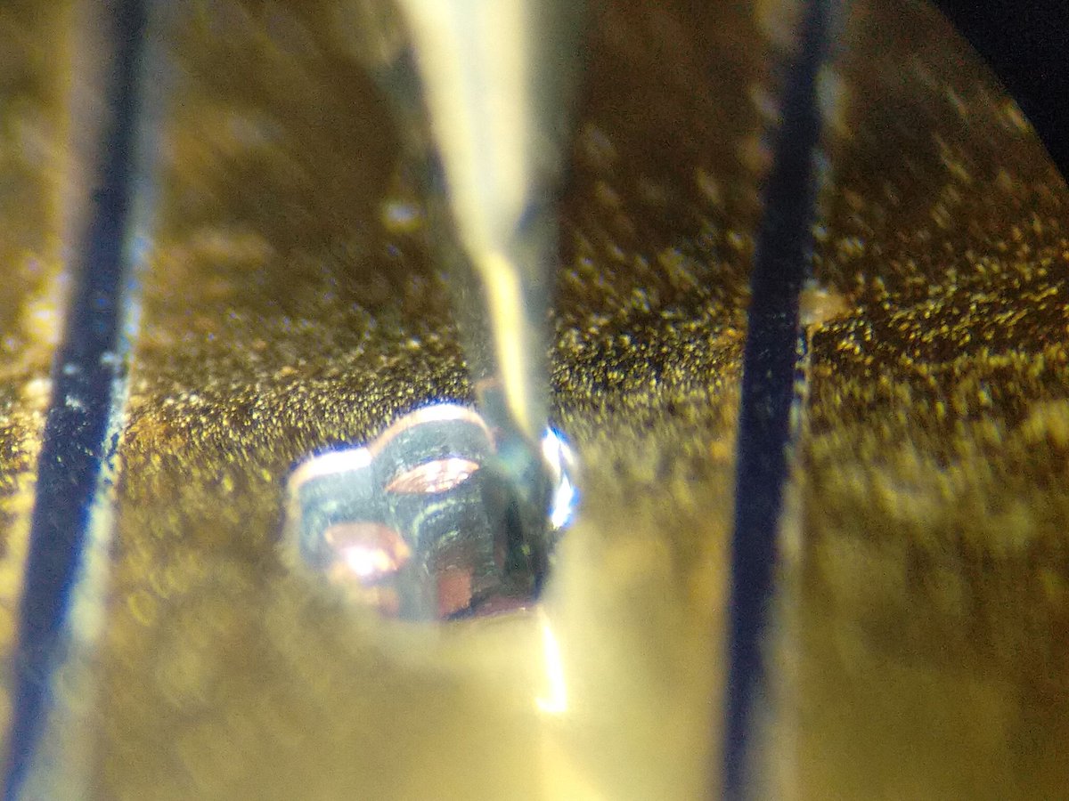
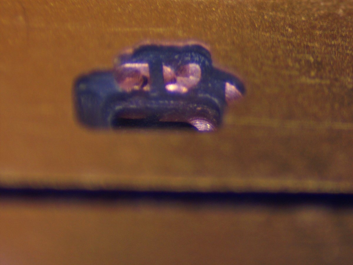
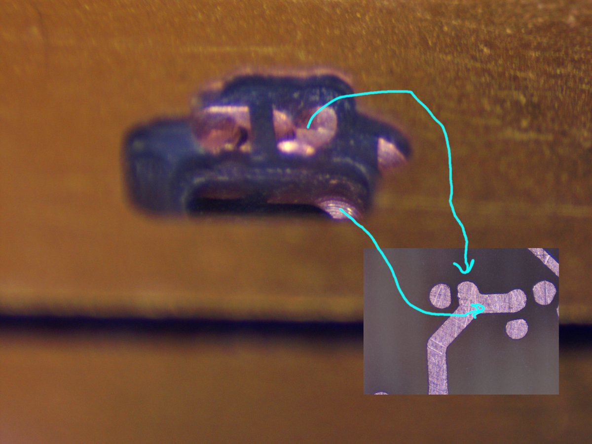
Annotated so you can see the various structures better.
It looks like the diagonal trace is cut around the knee, but not separated from the via pad. So I have to fully break that, then expose the other end and reconnect it.
It looks like the diagonal trace is cut around the knee, but not separated from the via pad. So I have to fully break that, then expose the other end and reconnect it.
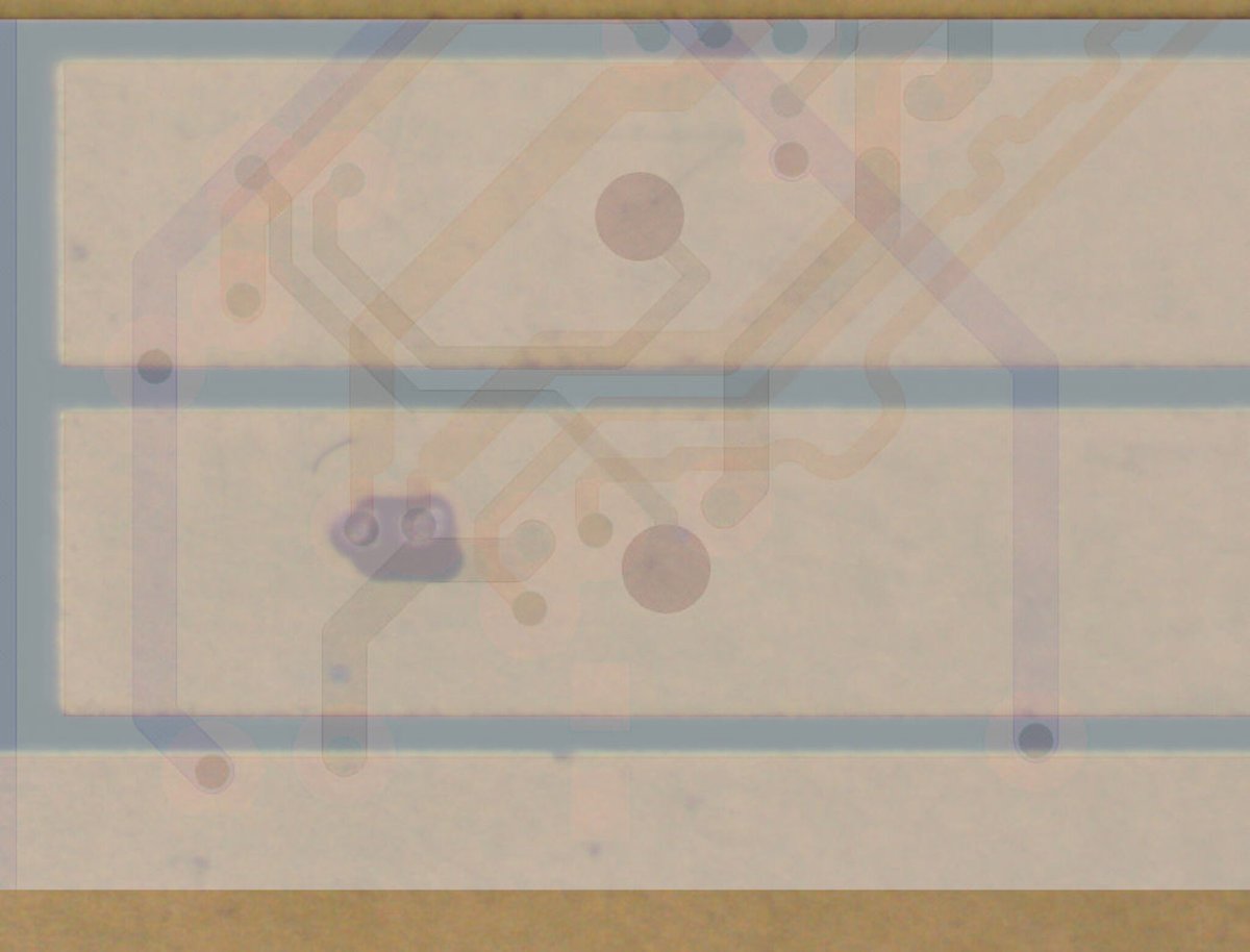
And here's the old top down microscope+gerber overlay view. The trace we're grazing at the right side of the cut is the orange trace just right of the hole in this image.
Top down view after the next milling operation. We're a few μm above the copper at each end of the trace. Can probably do the rest by hand with a scraper and scalpel.
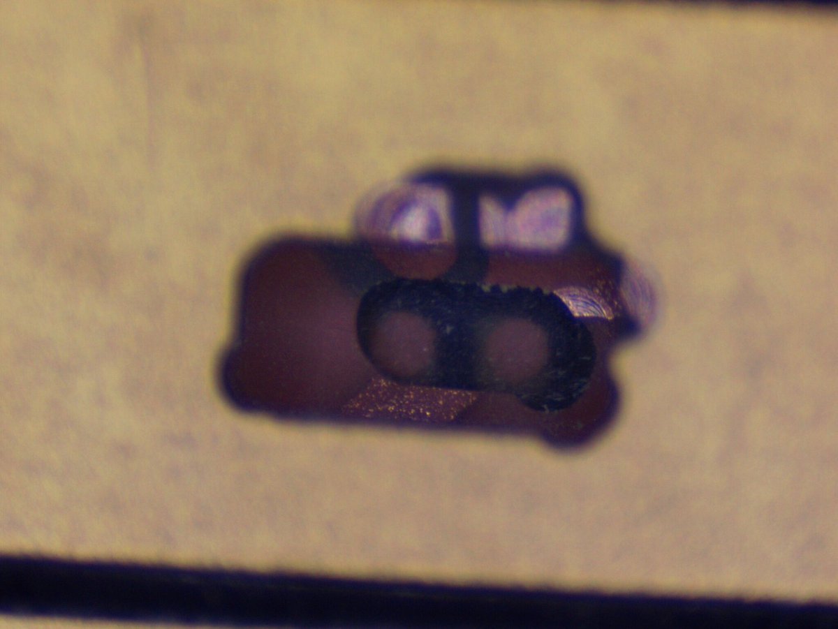
On second thought, no - I need to go just a tiny bit further up to make sure I can see the point of short.
Angled view. I need to go probably another 50-75 um up on the top right corner.

After a few more milling steps.
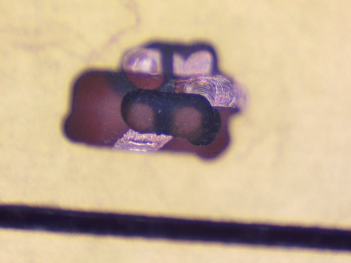
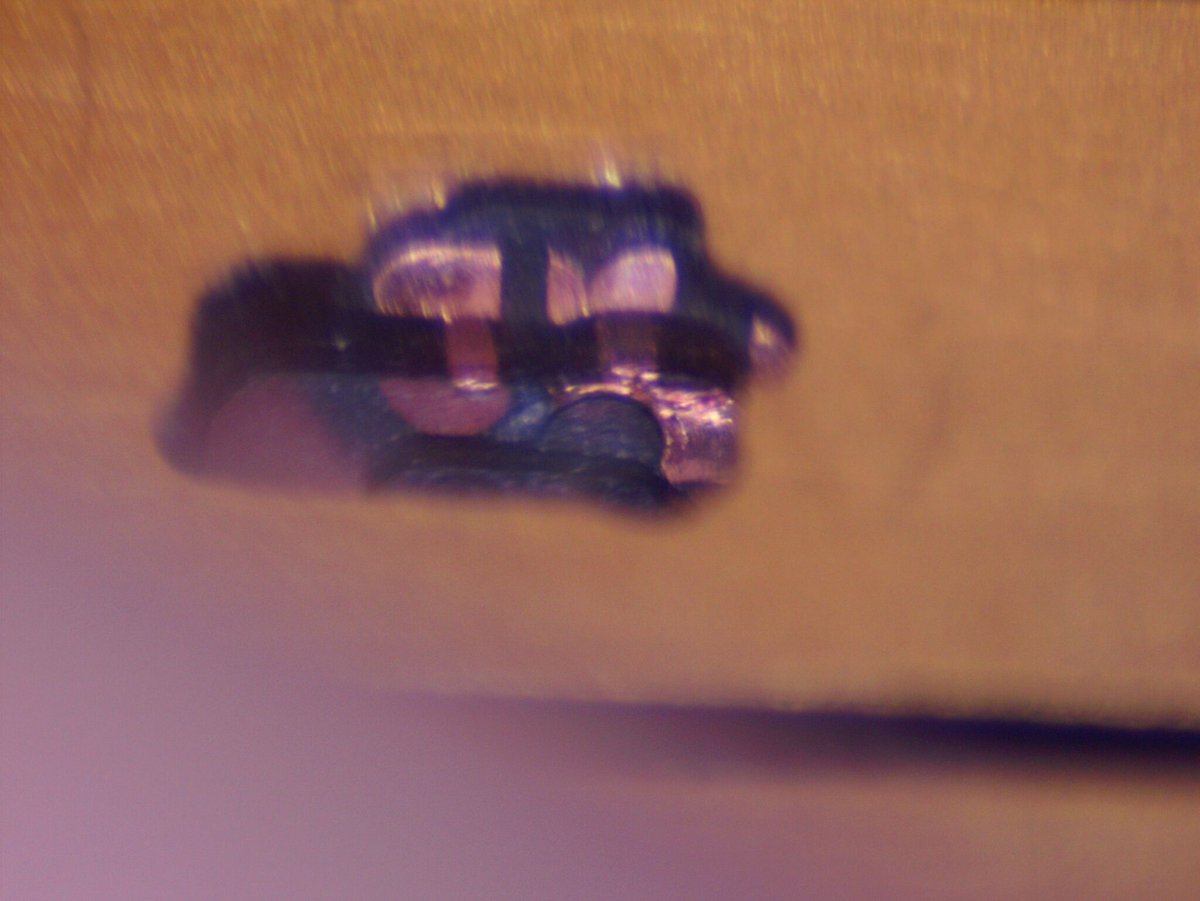
A bit of careful work with a #11 scalpel and the short appears to be cleared, confirmed by continuity test.
I need to do some more careful probing to verify I didn't break anything else, then reconnect the cut trace and we're done...
... with the easier of the two edits.
I need to do some more careful probing to verify I didn't break anything else, then reconnect the cut trace and we're done...
... with the easier of the two edits.
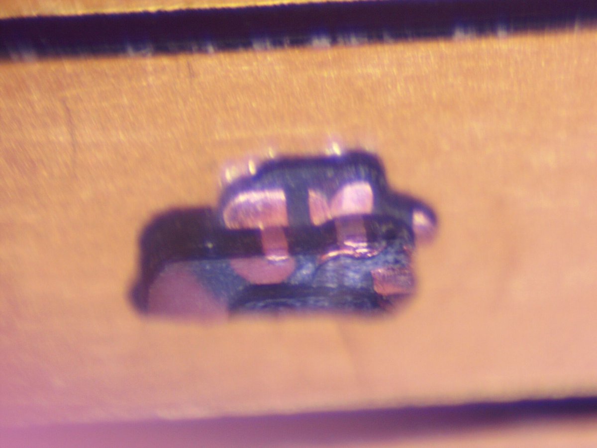
Just so we don't lose perspective, here's the full board prior to the soldering operation. That's a USB 2.0 connector.

Next step: use this giant oil pipeline to squirt some flux into the hole...
Wait a minute, that's a 22 gauge needle. And it won't fit.
Wait a minute, that's a 22 gauge needle. And it won't fit.

Switching to a 34 gauge needle, the smallest one I have in inventory, got the job done.

After tinning the two pads (and getting a bit of solder on the surface - not a big deal, we'll need to touch up the USB pad when we're done anyway)


And the bodge is done! Can you see it?

One last step before we wrap up - the hole needs to be free of flux residue so we can backfill with epoxy. Also makes for better photos.
Needless to say my swabs won't fit. So I cleaned it out with a 34 gauge needle, 3 ml syringe, and some acetone to "power wash" the area.
Needless to say my swabs won't fit. So I cleaned it out with a 34 gauge needle, 3 ml syringe, and some acetone to "power wash" the area.

Continuity checks pass - the short is gone and the cut trace is reconnected.
Next step is to fill with epoxy - I'm using AA-Bond 2104. As a glass filled epoxy material, it should have similar mechanical and electrical properties to FR-4.
Next step is to fill with epoxy - I'm using AA-Bond 2104. As a glass filled epoxy material, it should have similar mechanical and electrical properties to FR-4.
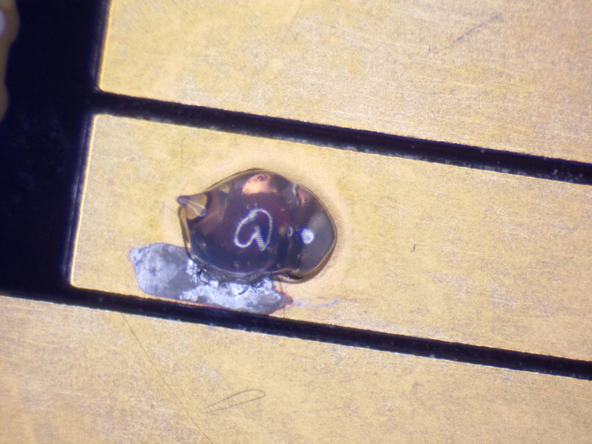
Once the epoxy is cured I can mill the surface flat (also removing the excess solder on the top layer) and, if it seems necessary, repair the USB connector pad.
(hi Hackaday folks! It's not over yet...)
The next step was to trim off the excess epoxy and some copper around the repair, so I can repair the USB pad. I used a large 1.5mm endmill for this.
The next step was to trim off the excess epoxy and some copper around the repair, so I can repair the USB pad. I used a large 1.5mm endmill for this.

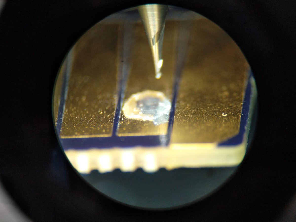

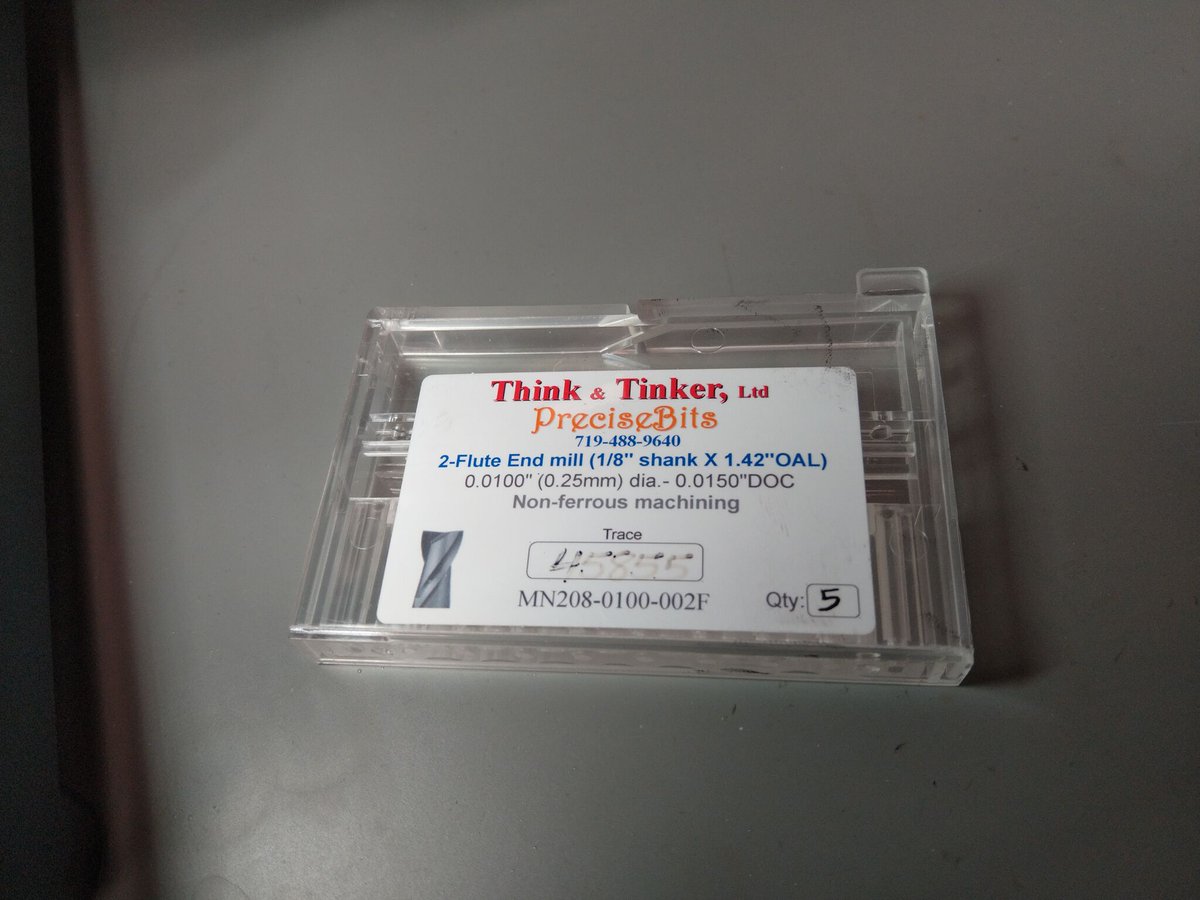
Here's a few shots of the tooling used for the milling portion of the repair. Just a benchtop mini-mill and a fairly generic stereo microscope, plus some ludicrously tiny endmills.


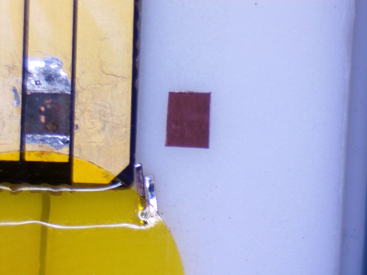
I selected the new copper pad from one of my library of "circuit frames". These are dry film adhesive backed copper foil cut into various shapes.
I ended up using a different one than pictured that had a rectangular trace pretty closely matched to the USB pin.
I ended up using a different one than pictured that had a rectangular trace pretty closely matched to the USB pin.

They do come in ENIG as well, but the tin plated ones are much less expensive (double vs triple digit prices) so I normally stock those.
Once the piece is cut to size, I removed some of the adhesive from the ends where it was going to overlap the main copper pads.
If I wanted to be extra fancy I could have milled this (and the corresponding spot on the PCB) but that seemed overkill for a prototype.
If I wanted to be extra fancy I could have milled this (and the corresponding spot on the PCB) but that seemed overkill for a prototype.
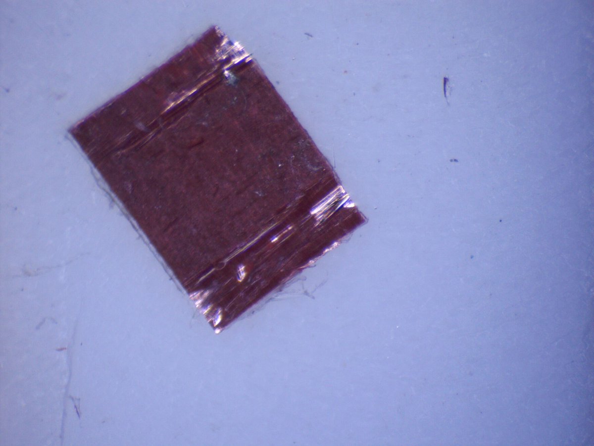
The adhesive is heat activated, so I usually just press it firmly into place with a soldering iron then give it a few seconds.
Once it cools, you can solder like normal (but you have to be careful not to dislodge it as the glue melts).
Once it cools, you can solder like normal (but you have to be careful not to dislodge it as the glue melts).
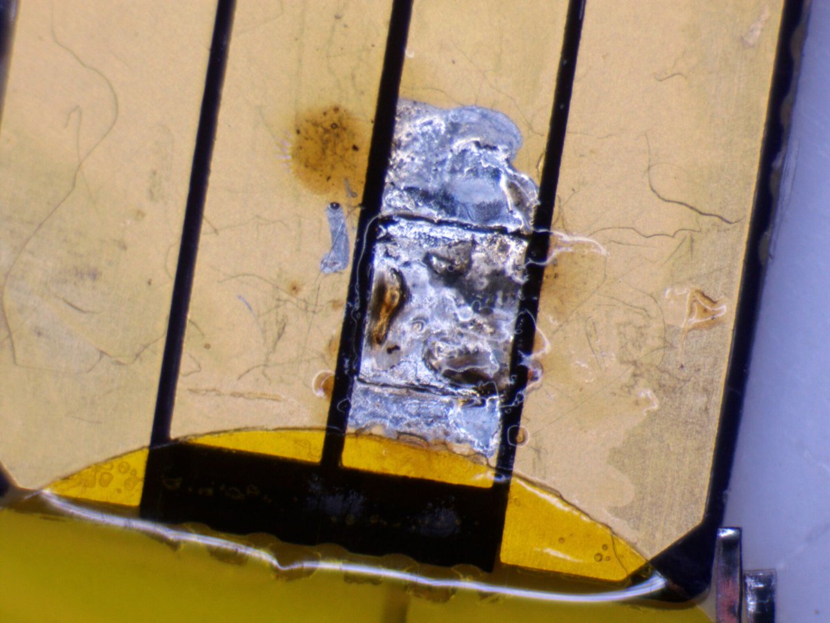
I spent a minute or two tweaking the solder finish to provide smooth rounded fillets on the ends of the repair (so it wouldn't snag on the USB port) and removing extra flux.
And this repair is finished!
And this repair is finished!


• • •
Missing some Tweet in this thread? You can try to
force a refresh