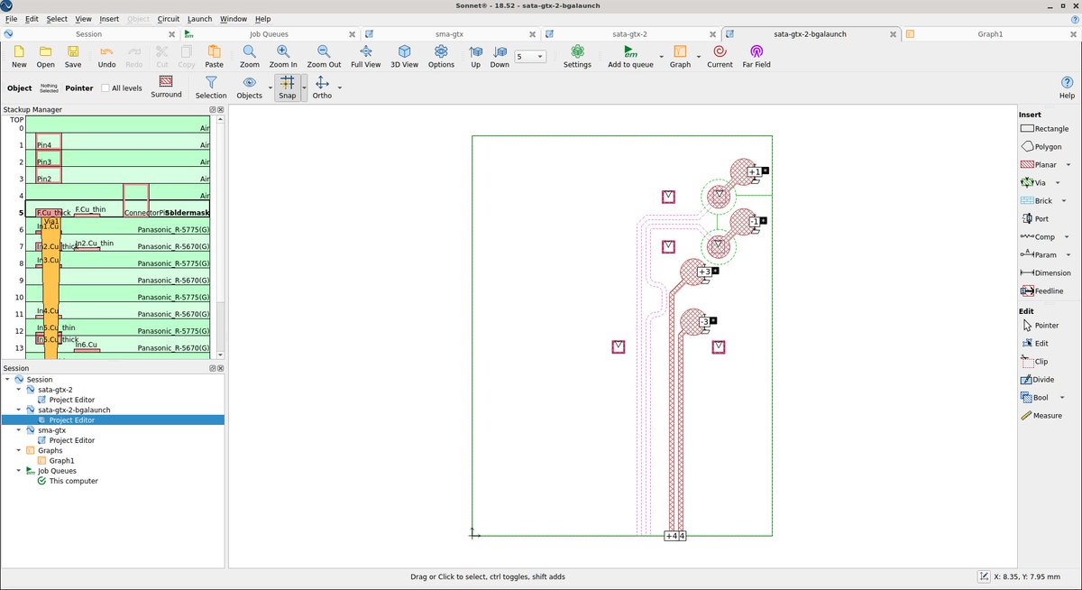
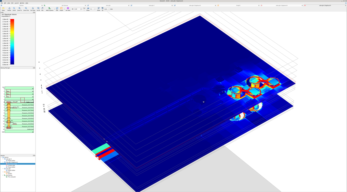
Finally got a decent EM simulation on the SATA pairs done. Only took four days... seems I need to simplify it further still.
Let's take a look at the results.
Here's insertion loss. S21 (red), is the left pair going through the layer change, S43 (blue) is the right pair with no layer change.
Looks like the layer change is introducing some kind of impedance mismatch.
Neither one really has great return loss, but the pair with the layer change is definitely a lot worse.
TDR transform on the two pairs (different Y axis scales).
Seems to suggest that the impedance on the back layer pair is way high, which makes no sense at first because the stackup is symmetric land I have stitching vias everywhere I should...
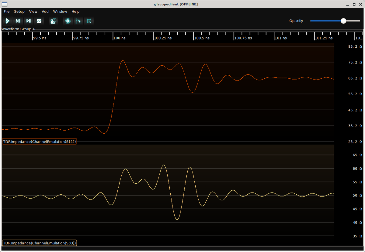
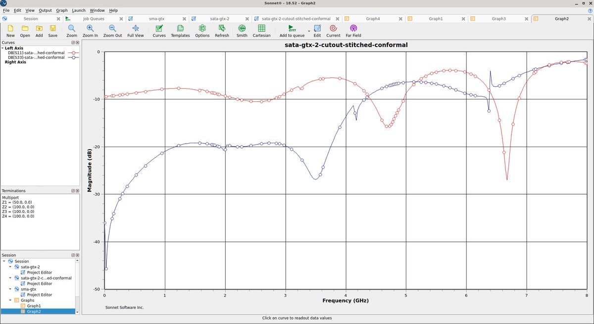
This is interesting. Simulating just the BGA launch in isolation shows uniformly terrible S11 and fairly decent S33.
I wonder if there's something to be learned from this...
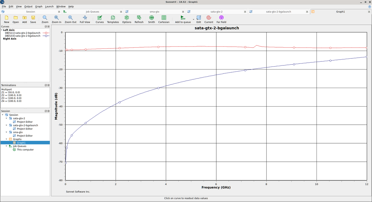
Wut?? TDR transform of S11 is showing about 75 ohm impedance for what should be a 100 ohm line/
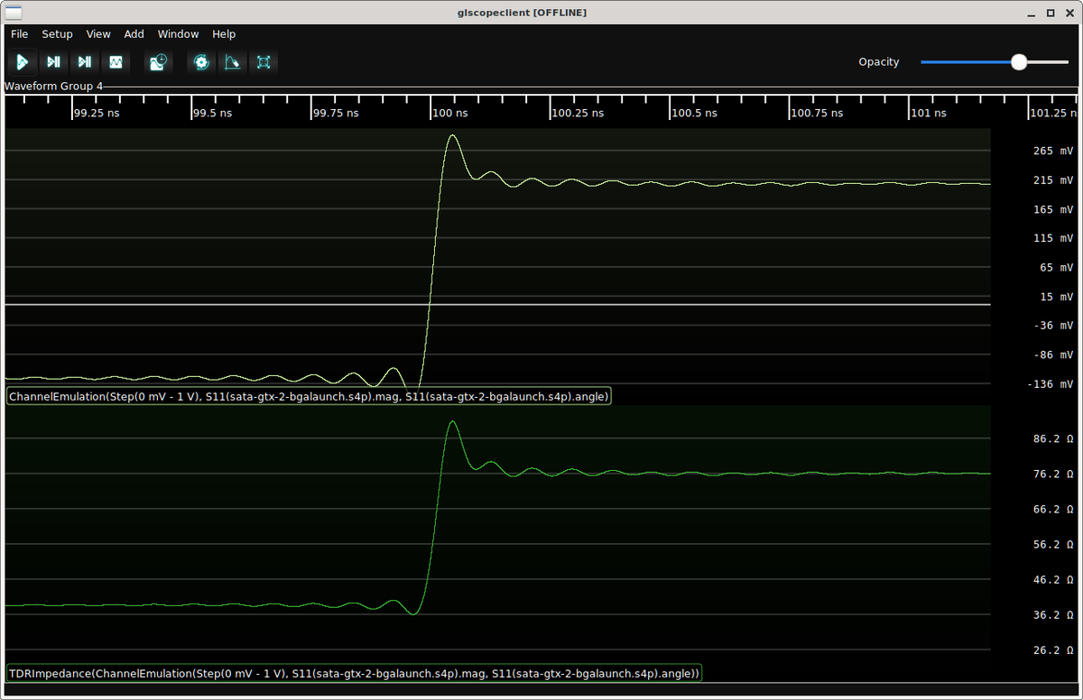
Derp. Had port impedance set wrong. That would explain a lot.
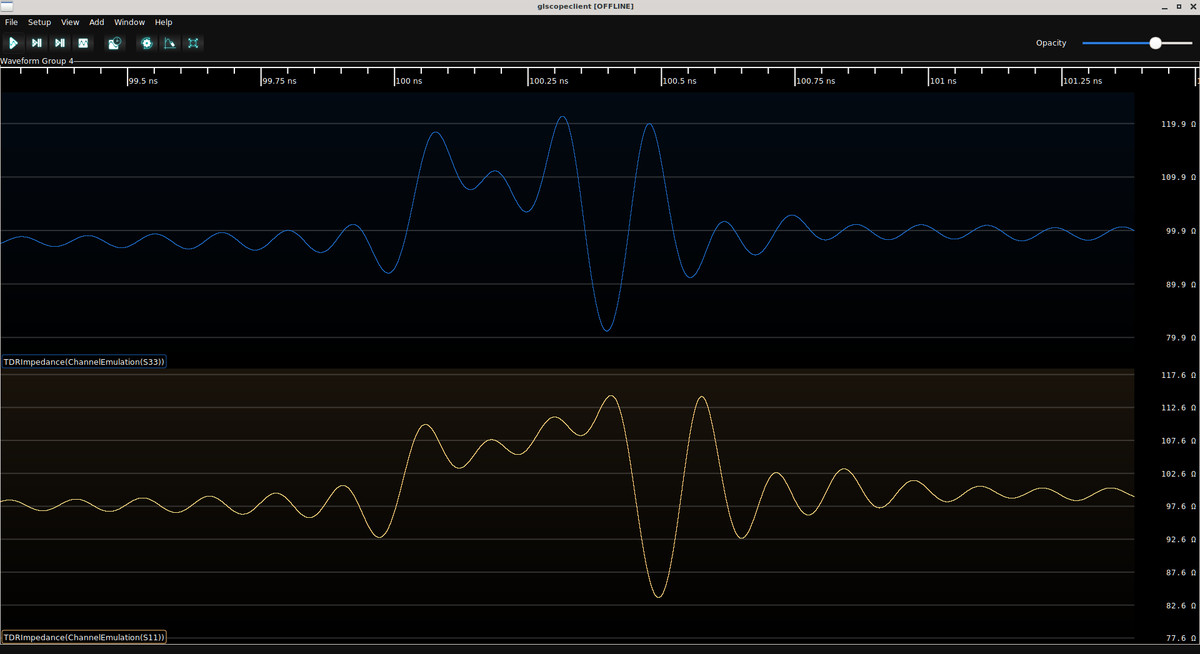
S-parameters and TDR transform of the two pairs with corrected impedance. Makes a lot more sense now.
I'd like to tune both further but the graphs are plausible.
• • •
Missing some Tweet in this thread? You can try to
force a refresh

Assembled the (v0.6) AKL-AV1 prototype! Characterization results in this thread.
For those of you just tuning in, the AV1 is an open hardware 1.5 GHz class, high impedance, solder-in, single ended active voltage probe (5MΩ || 350 fF, 10x attenuation) that runs on 5.5V DC.
First step is low frequency trimming. This adjusts the DC path (OPA210) and AC path (BUF802) to have the same gain.
Seen here before and after.
Next, high frequency trimming. The JFET amplifier stage has a 2.4 pF input capacitance so to reduce loading on the DUT there's a 5:1 R-C divider in front of it.
Shunt path is a 1MΩ terminator across the BUF802, series path is 4MΩ in parallel with a 250 - 750 fF trim cap.
Friend of mine has been troubleshooting some major EMC problems for a while so I decided to grace the project with a song. Here's my latest draft. Suggestions?
"The Sound Of Crosstalk"
(to the tune of The Sound Of Silence)
Hello crosstalk, my old friend
I've come to fight with you again
Because a field line softly creeping
Left microstrip while I was testing
And the waveform I was sending through my board
Still remains... it is the sound of crosstalk
In restless days I probed alone
Nearby striplines, coupled tones
'Neath the halo of a H-field loop
I turned my specan to the board and hoped
When my graphs were stabbed
By the peak of a coupled tone
Standing alone
It was the sound of crosstalk
This is how you're supposed to simulate a circuit with a resistor in it, right?
Device is a R20L125 rod resistor from ResNet Microwave (electrotechnik.com/pdf/ROD.pdf). I'm interested in simulating the flatness of a probe using it as an attenuator.
Vendor doesn't publish S-params.
This model is mostly based on guesswork as I don't have a lot of details from their datasheet on internal construction (e.g. metal layer thicknesses).
But as a first order estimate, I calculate 7-10 fF shunt capacitance depending on frequency.
I asked for samples, and they're going to be sending me two 50-ohm devices.
My hope is that with some EM simulation plus characterization of the 50-ohm parts, I can extrapolate to see how a 450-ohm device behaves.
I've had an HP LaserJet all-in-one printer in my home office for a couple of years now. I finally ran out of black toner and had to swap the cartridge out.
The box had this cool anti-counterfeiting seal on it, which changes appearance as you tilt it. Let's take a closer look!
There's a barcode and QR code that seem to be printed using fairly ordinary black ink on paper, and then there's a special insert (the blue area) where Magic(tm) happens.
Let's look at the "toner" microprint area.
As you tilt the label, the six little balls rotate while the rest of the graphic remains fairly constant in appearance.
Open offer: If anyone sends me one of these (or any other similar audiophool products) I'll do a full signal and power integrity workup on it. And send it back after if you want.
I'd love to see how awful that "low noise" power rail really is.
Oh, and of course these geniuses are throwing a fancy TCXO on the board to get "low jitter" clocking.
... except the actual NVMe interface is clocked by the PCIe refclk. Which is spread spectrum modulated on most motherboards.
So even if the flash controller's internal PLL had good enough jitter characteristics that a better reference would improve it, at most you'll improve setup/hold margins between the controller and the NAND die.