
In this thread, I will try to teach you about a RISC-V processor, piece by piece! You can take a look at the image that depicts the instructions and registers of an RV32I (simpelst) and ask questions before we gradually delve into the design. #riscv #twitterSchool 1 

Oh, I forgot about the registers! Registers are memory in the CPU. They range from x0 to x31. A register has 32 bits in RV32I. The content of x0 is always zero, but we'll get to that later. The registers also have other names (on the right). But let's ignore that for now. 2

In RISC-V, there are many extensions and designations, including 64-bit and 128-bit. But we will ignore that and not go into it. However, there is a little sweet brother RV32E, which has only 16 registers instead of 32. Look here, but ignore it for now.
five-embeddev.com/riscv-isa-manu…
3
five-embeddev.com/riscv-isa-manu…
3
It would be very helpful to understand the instructions and be able to write assembler programs, wouldn't it?
4
4
Let's simply compute x3 = x4 + x5.
Regardless of what is already stored in x4 or x5.
It's simple, we happen to have registers named x4 and x5. And RISC-V is a 3-address computer, with one target and two operands. How cool!
5
Regardless of what is already stored in x4 or x5.
It's simple, we happen to have registers named x4 and x5. And RISC-V is a 3-address computer, with one target and two operands. How cool!
5
The instruction would simply be 'add x3, x4, x5'. And the instruction is of the R-type, because only registers are involved. So, that's it for today. Try playing around with the instructions!
6
6
Why RISC-V? I suspect that this architecture will play a big role until silicon has reached its limits.
I have implemented the three most important basic designs: multicycle, single cycle, and a 5-stage pipeline. In this thread, I am trying to explain the single cycle CPU, which also exists in the GitHub directory for download.
7
7
I allowed myself the fun of running my single cycle CPU at 80MHz, which corresponds to 80 million instructions per second. That was a very nice experience. The bottleneck is the UART, which transmitted data at 3MBaud.
8
https://twitter.com/splinedrive/status/1627036278821732352
8
The single cycle CPU can be found here. I will explain the concepts of the different types later
github.com/splinedrive/ki…
9
github.com/splinedrive/ki…
9
A small comment.
I may be a bit naive because I have only been coding for 2 years, but for me, CPUs must be in Verilog and, if necessary, in VHDL. I don't want to use or look at anything else.
I may be a bit naive because I have only been coding for 2 years, but for me, CPUs must be in Verilog and, if necessary, in VHDL. I don't want to use or look at anything else.
Hello everyone, I am currently missing a word to see how simple the structure of a RISC-V processor is. Could you try out my C emulator for an RV32I? You will get to enjoy MicroPython. Yes, you heard that right!
clone it, make it, run it, micropython it!
github.com/splinedrive/ki…
clone it, make it, run it, micropython it!
github.com/splinedrive/ki…

My not yet released emulator also boots Linux.
https://twitter.com/splinedrive/status/1627108161499848704
Here, you can observe the exact assembly instructions that the CPU is executing. It's simply beautiful to watch.
10
Let's get back to the CPU commands. A classic CPU has the following types of commands that can be categorized: logical commands, arithmetic commands, transport commands, and control commands.
11
11
Von Neumann defined the principle of the CPU in 1945 with the following points:
Memory: Data and instructions are stored here.
CPU: It consists of a control unit and arithmetic unit that execute the categorized commands described in 11
12
Memory: Data and instructions are stored here.
CPU: It consists of a control unit and arithmetic unit that execute the categorized commands described in 11
12
Input/Output (I/O): Communication with other hardware components.
Buses: They facilitate communication between different hardware components.
13
Buses: They facilitate communication between different hardware components.
13
There is also the Harvard architecture, which was developed in the 1940s as well. The main difference is that instructions and data are stored in separate memories. This separation increases performance by allowing simultaneous access to both types of memory.
14
14
In the thread, I mentioned the three classic approaches to computer architecture: single-cycle, multi-cycle, and pipelined CPU architecture. Single-cycle and pipelined architectures utilize the Harvard architecture, while multi-cycle architecture employs the von Neumann arch.
15
15
That was a bit too abstract. Here are two images taken from Wikipedia for Harvard and Neumann architecture.
Read this through, it's very interesting.
en.wikipedia.org/wiki/Von_Neuma…
en.wikipedia.org/wiki/Harvard_a…
16
Read this through, it's very interesting.
en.wikipedia.org/wiki/Von_Neuma…
en.wikipedia.org/wiki/Harvard_a…
16


@jangray had messaged me, he still has some comments regarding Neumann and Harvard. It's an honor to have you commenting here.
In this thread, I am only expressing my understanding. It's possible that I may be wrong, so please correct me. I'm just a hobbyist in logic design who loves to control bits. And I'm sharing my experience of the last 2 years.
Let's come back to the instructions we saw at the beginning. Play around with them! I can recommend this online simulator for you!
That helped me a lot. I think logic design of a CPU without understanding instructions doesn't make sense.
cs.cornell.edu/courses/cs3410…
17
That helped me a lot. I think logic design of a CPU without understanding instructions doesn't make sense.
cs.cornell.edu/courses/cs3410…
17
This is really fun and you learn a lot. Take a look at the CPU registers! Learn assembly language, that's the only way you can understand the CPU.
18
18
I hope you have familiarized yourselves with the instructions in the simulator.
All algorithms and computer programs are mapped onto these few commands. I find it incredible to get Micropython running on the small emulator, where a RISC-V machine is being simulated.
19
All algorithms and computer programs are mapped onto these few commands. I find it incredible to get Micropython running on the small emulator, where a RISC-V machine is being simulated.
19
Let's start the demo and enjoy RISC-V being emulated with Micropython. You can download my emulator here, I think it's really crazy.
github.com/splinedrive/ki…
github.com/splinedrive/ki…
20 🖕
The emulator is actually written in C, but it somewhat represents how I approach things in Verilog. This applies to all the processor types I have implemented in a similar way.
21
21
You should study this program a little, then we'll go through the commands individually again. The command structures, types or categories. Then we can move on to concrete register transfer and discuss the components.
22
22
I would have taken the same approach, but I went through the hard school of trying things out on the FPGA without simulation, since I had no idea what was possible two years ago. You must get a feeling for what is being generated in the synthesis.
23
23
I repeat, we are taking an RV32I. It is a 32-bit RISC-V processor, but there are also 64-bit and 128-bit versions available. A simple processor fetches 32-bit instructions, as you can see in this image. These instructions represent various command types.
24
24

Let's start with R-type. The instruction only fetches operands from registers and writes the result back to a register. As I mentioned, RISC is mostly a 3-address machine. The format is Target register, Operand1 Operator Operand2. See the table below.
25
25

Now let's move on to the immediate instruction. It's similar to the R-type instruction, but the second operand is not fetched from a register. Instead, it is obtained from the instruction itself and is 12 bits long, representing an
26
26
unsigned value from 0 to 4095. For example, 'addi x1, x2, 5', where 5 is embedded in the instruction.The format is Target Register, Operand1 Operator Operand.
In the case of a non-load instruction,
26
In the case of a non-load instruction,
26
the load instructions are also immediate instructions, but they read from external memory instead of registers.
The immediate value is added as an offset value to a register that serves as a pointer in memory to read.
c-syntax: target R = *(RS1 + imm)
27
The immediate value is added as an offset value to a register that serves as a pointer in memory to read.
c-syntax: target R = *(RS1 + imm)
27

The S-type instruction. It is used for write operations on external memory, so no registers are involved as target. The same concept applies here: we have a register as the base and an immediate value as the offset, which are added together.
c-syntax: *(RS1 + imm) = RS2 28
c-syntax: *(RS1 + imm) = RS2 28

With load/store operations, there are different variations based on the data types being operated on, but we will discuss those later during the implementation.
29
29
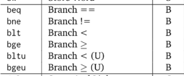
The next instructions are the B-type ones. They are used for conditional branching, which helps to implement if, else if statements.
The same concept applies here: when the condition is true, jump to the program counter plus the immediate value.
30
The same concept applies here: when the condition is true, jump to the program counter plus the immediate value.
30
Wait, but the immediate value can allow jumping both forward and backward by handling positive and negative offsets. We will discuss more about this during the implementation.
31
31
Before we move on to the other two types, you can take a look at my RISC-V compiler. It will help you understand how to use the instructions in a high-level language.
github.com/splinedrive/le…
github.com/splinedrive/le…
32 🖕
We specifically apply the positive/negative offset to other instructions as well. I will showcase Verilog passages for this purpose.
I forgot to mention one instruction that uses immediate format. Jump and link Register. It executes code from Register plus immediate value.
PC = RS1 + Imm. You can manage absolute jumps with it!
PC = RS1 + Imm. You can manage absolute jumps with it!

The next instruction is jump and link. It jumps relative to the program counter with an immediate offset forward or backward. This realizes relative jumps and is stored in the J-format.
33
33

PC = PC + IMM
With the 20 bits, one can jump relatively far and use, for example, Linux on my SoC (System-on-a-Chip) to avoid using MMU.
github.com/splinedrive/ki…
With the 20 bits, one can jump relatively far and use, for example, Linux on my SoC (System-on-a-Chip) to avoid using MMU.
github.com/splinedrive/ki…
Now we have reached the last type which is U-type. Here, 20-bit immediates are stored, which are shifted 12 bits to the left. You can combine this with an immediate 12-bit instructions. The next comment provides clarity for the pseudo-commands 'la' and 'call'.
35
35

In summary, auipc is used to set up a 32-bit address that is then used with another instruction to access data or code that is located outside the current program counter range. lui is commonly used in combination with 'addi' to load a complete 32-bit value into a register.
36
36


So now we have described all RV32I instructions and can run MicroPython on it using my emulator. Please take a look and understand it before we move on to the Verilog design.
37
https://twitter.com/splinedrive/status/1651627428685520907
37
We have now gone through all of RV32I and it is now possible to unroll .
@threadreaderapp unroll
@threadreaderapp unroll
Here are a few anecdotes before we continue.
My first CPU was one that could even perform multiplication and division. It was a freestyle project, and I didn't have much knowledge about what a synthesizer does.
38
My first CPU was one that could even perform multiplication and division. It was a freestyle project, and I didn't have much knowledge about what a synthesizer does.
38

Therefore, I abandoned the concept and completed the computer architecture course from Harris on @edXOnline , and understood what logic design is all about. edx.org/course/compute…
39
39
Also, it is recommended to try to work structurally (instances) and describe the lowest nodes behaviorally so that you can get nice RTL images and maintain an overview for extensions.
40
40
So, I would say let's start with a processor. I'll take my emulator as a basis. I don't think there's any point in discussing every bit, you have to take a look at it yourself. I'll just show the direction and the semantics.
github.com/splinedrive/ki…
41
github.com/splinedrive/ki…
41
We had discussed the types and some specific instructions, which can be determined based on the opcode that is 6 bits wide. Take a look at the instruction format table and the enums from the C code. 42


Once we have figured out which instruction we have, we can then assemble our immediate values.
In Verilog, bit manipulation is much simpler than in C.
I assign the task of studying this code.
43
In Verilog, bit manipulation is much simpler than in C.
I assign the task of studying this code.
43


The little C code emulates an RV32I RISC-V processor that runs the new version of MicroPython. I find it crazy. The code represents a bit of the approach that I also use in hardware.
44
44
In the end, we built a bit of a decoder structure, but there's still something missing, but that's for later.
45
45
It's easy to lose track here. Before we can do that, the 32-bit instruction must first be fetched from memory and then examined for patterns.
46
46
Small note, if I use the RTL of a single-cycle RISC-V CPU, then we are right where I have highlighted everything in red. "Extend" is basically the unit that extracts the immediate value based on the instruction type. The instruction comes directly from memory.

The one-cycle CPU executes one instruction in one clock cycle. However, it has many boundary conditions, which we will discuss later on.
In digital circuit design, register-transfer level (RTL) is a design abstraction which models a synchronous digital circuit in terms of the flow of digital signals (data) between hardware registers, and the logical operations performed on those signals.
en.wikipedia.org/wiki/Register-…
en.wikipedia.org/wiki/Register-…
If we are already in the process of decoding the command based on the bit pattern, then we can continue. We will also determine what category of ALU operation the command has or should have. See the excerpt from the emulator.
47
47
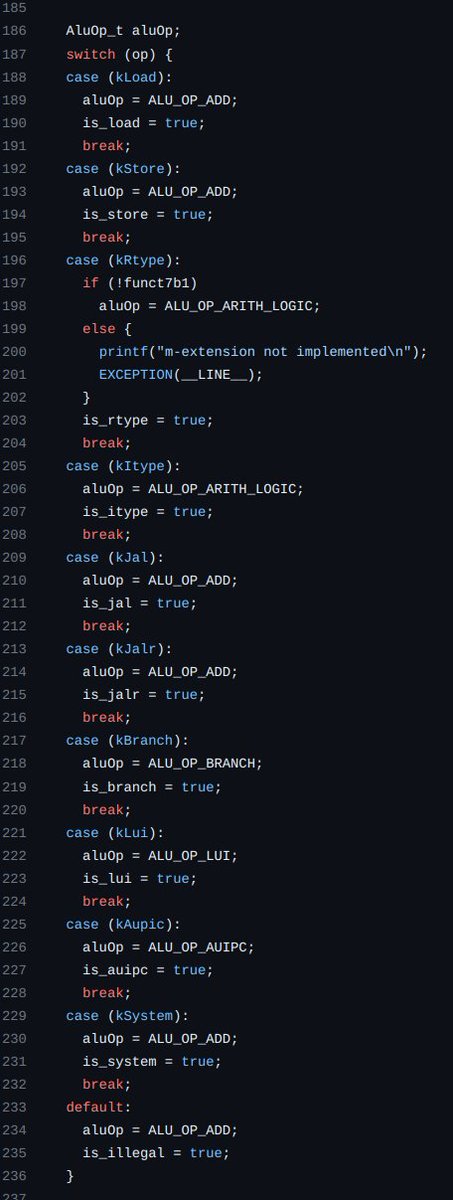
Now we come to the part that refines the commands regarding ALU operations. Bit patterns are compared again. In Verilog, I do it almost analogously.
48
48

Everything before was the decoding phase, now we come to the so-called execution. This is the so-called Arithmetic Logic Unit.
49
49

Oh, how nice, now we have our memory operations: load/store.
50
50

Now we come to the part that is nicely called writeback. Here, the result of load or ALU operations, or other values, are written back into a register.

I had forgotten the code for fetching a command, the so-called fetching.
51
51

of course, we also need to recalculate the program counter depending on what we have - branches, jumps, or sequential processing of commands.

In every CPU variant, no matter what type, we always have the same sequence: fetch -> decode -> execution -> memory -> writeback. Always this progression, one must burn it into their brain.
52
52
Now we can enjoy it before we move on to a concrete hardware implementation.
53
53
You'll never learn it if you haven't implemented it from scratch yourself, as a tip. You have to go through the struggle.
54
54
Once you've understood it, it feels like kindergarten.
55
55

Now we come to a concrete hardware implementation in Verilog. In the video, you can see how I clone my repository and start the simulation to calculate a ray-traced image.
56
56
A so-called single-cycle CPU. All phases are executed in one clock cycle. This is done theoretically, as abstracted in my emulator. I will get to the meaning and relations of multicycle and pipelining later.
57
57
https://twitter.com/i/status/1579589541677371395
I synthesized this CPU in a Vivado project and waited for 3 hours. I managed to achieve 80MHz, which means 80 CPI (cycles per instruction). That's 80 million instructions per second. It's like Hellraiser style.
58
Of course, I did this on my @DigilentInc Genesys 2, which cost me 1,300 Euros. It was worth it to me.
Actually, I bought it just for that reason.
Actually, I bought it just for that reason.
Oh, so the operand registers and the destination register are encoded in the bits of the instruction, depending on the type. But you can figure that out for yourself by looking at the instruction format. Maybe now you can understand more about what the picture means.

I had a feeling that something like this was possible. I love large combinational logic.
That was my foundation, it was great. The book is also highly recommended.
You need to have the right books or the right materials to set the right course.
pages.hmc.edu/harris/class/e…
You need to have the right books or the right materials to set the right course.
pages.hmc.edu/harris/class/e…

I compiled the links for my Verilog implementation and the material for the single-cycle CPU from Harris here.
github.com/splinedrive/ki…
pages.hmc.edu/harris/class/e…
59
github.com/splinedrive/ki…
pages.hmc.edu/harris/class/e…
59
❤️❤️❤️❤️❤️❤️❤️❤️❤️❤️❤️❤️❤️❤️❤️❤️❤️❤️❤️❤️❤️❤️❤️❤️❤️❤️❤️❤️❤️❤️❤️❤️
I love huge combo logic!
I love huge combo logic!

Has the course been helpful so far? Should I still explain my single cycle CPU with pictures and code passages? If not, I'd rather just code :)
I don't want to go into the details of bits, I find it pointless. People have to figure it out themselves. I'm just showing the direction.
fuck you people, karma will catch up with you.
Before I go to sleep, let's slowly start discussing my one cycle CPU, where everything happens simultaneously. We'll gradually explore what this means. I'll explain the other types of CPU approaches at the end of the chapter.
60
60
In essence, one cycle is a huge combinational circuit, and the memory from which you read or write must also be capable of doing this in a single clock cycle.
61
61
This is what my CPU looks like from the outside, with which I managed to achieve 80 MIPS and output a raytracer via UART.
62
62

The single-cycle CPU is a Harvard architecture. The instruction memory and data memory are separate, and both can be accessed in parallel within a single clock cycle. The ALU result is the address for the data memory, and the PC is the address for the instruction memory.
63
63
instr[31:0] is the data word from the instruction memory, readdata and writedata are associated with the data memory, and writemask is used to modify one of the four bytes in a 32-bit data word, depending on the type of store instruction.
64
64
clk is the clock signal, and resetn is used to reset the processor.
1, 2, 3 Gute Nacht
64
1, 2, 3 Gute Nacht
64
There is more at the weekend.
Let's take a look inside the processor. Oh man, what's this: control_unit and datapath_unit. It looks kind of cool.
65
65

The control unit generally controls the memory access for data and instructions, as one can see from the interface. It generates control vectors for the ALU, other involved UNITs and the multiplexers, essentially directing the data flow in the data unit.
66
66
That's how it looks inside the controlunit! Actually, the processes are similar to those in my emulator written in C. You can take a look at it for better understanding.
67
67

The main_fsm (finite state machine) implements all control vectors necessary for the entire process.
68
68

That's how it looks inside the data unit. It consists of the registers, ALU, multiplexers, PC counter, all of which are controlled by the control unit during the process.
69
69

See how beautiful the ALU is. It implements the arithmetic operations and the control unit instructs it on how to handle the operands.
70
70

Here's the register file: 2 operands, one target => 3-address computing machine, typical RISC architecture.
71
71

In single cycle, that's essentially just one state. And it can be referred to as a decoder.
All in one clock cycle!
Decode the instruction, get the data from the reg or from the data memory, compute it and write it back into the register or memory.
72
Decode the instruction, get the data from the reg or from the data memory, compute it and write it back into the register or memory.
72
Keep in mind, RISC is based on load/store. This means, first load into register, then manipulate and you can only write back one register into memory.
73
73
In a multicycle CPU, this happens over several cycles, to utilize resources such as the ALU multiple times, depending on the state of the CPU. That's cool, you can make very small designs with it.
74
74
Like my Linux SoC on the iCE40HX8K, a real hardware implementation, no tricks. An RV32IMA SoC. First Linux SoC on HX8K.
75
75
https://twitter.com/splinedrive/status/1652973651019407361
The pipeline CPU is essentially a single-cycle CPU segmented, with registers inserted in between, where the data and control signals are stored in the meantime.
76
76
The registers work with one clock cycle. Depending on the depth of the pipeline, the first command requires as many clock cycles as the size of the pipeline.
After the pipe is filled, one instruction is processed per clock cycle.
76a
After the pipe is filled, one instruction is processed per clock cycle.
76a
Then there are so-called control and data hazards, but that's another chapter. They ensure that we don't process an instruction every clock cycle.
76b
76b
This divides the large combinatorial circuit, allowing the circuit to reach a stable state faster. This results in a higher clock speed. But physics put a damper on that.
77
77
It would actually be great if we could realize everything with large circuits without going through all this trouble.
78
78
I love pipeline CPUs, I hope to only work with them after the summer. Multicycle is closed for me. Maybe I'll design something for Hidden RISC if I want to give my fat processor a few assistants.
https://twitter.com/splinedrive/status/1583967446137860097
@threadreaderapp unroll
• • •
Missing some Tweet in this thread? You can try to
force a refresh


