[1/16] 🧵 A History of ASML’s Scanners
Enabling the AI Revolution with chip printers—the most complex machines ever built.
Enabling the AI Revolution with chip printers—the most complex machines ever built.


[2/16] The List
Here we have my list of all the ASML’s scanner models installed over the past 35 years. It’s not an exhaustive list; I’m sure I’ve missed a few, but it’s what I was able to put together based on the tools I’ve run (which is most of them) or models my friends have told me they’ve used. As you can see by the super small font I had to use here, it’s a big list of around 50 different tool models. Let’s do a deeper dive on this history in this thread and how we got to the latest EUV tools being installed today in the most advanced chip factories around the world.
Here we have my list of all the ASML’s scanner models installed over the past 35 years. It’s not an exhaustive list; I’m sure I’ve missed a few, but it’s what I was able to put together based on the tools I’ve run (which is most of them) or models my friends have told me they’ve used. As you can see by the super small font I had to use here, it’s a big list of around 50 different tool models. Let’s do a deeper dive on this history in this thread and how we got to the latest EUV tools being installed today in the most advanced chip factories around the world.

[3/16] Scanner Platforms
When we think of the different generations of lithography tools that have been developed over the years, we often associate each generation with the light source. Generally speaking, the smaller the wavelength of the source, the smaller the circuit patterns we can print. But in reality this is only part of the puzzle. The true ROI for a scanner—a fab needs to make money with these machines after all—can be distilled down to the overlay specification (Cols J-L) and the throughput (Cols N/P).
Overlay is how accurately the scanner can place circuit patterns on top of each other, and it's often the most important factor for chip yield, which directly affects the fab’s bottom line. Throughput is how many exposures per hour the machine can do; the more exposures, the better the ROI on the machine. With the latest EUV models costing about $400m each, getting more wafer exposures out of each tool directly affects a fab’s capital expenditure and production output.
The scanner platform is the basic frame of the tool and how it operates. A single platform contains various components like the source and lens, and different ones can be used to set the resolution of the machine; however, the platform type and the model iterations for each of them are how the overlay and throughput are improved. Ultimately the platform itself is the best way to drive ROI improvements of these machines.

[4/16] Scanner Platforms Continued…
ASML has developed 5 scanner platforms over the years, and each platform had a series of tool models released where iterative improvements were made to both the overlay and throughput such that fabs could get improved ROI on their lithography investments. Each new generation of the platform allowed for major leaps in the ROI.
PAS 5500 Platform:
This platform is what put ASML on the map back in the early 1990s, and these tools are still in use today and fully serviced by ASML. It was a single-wafer stage system (more on this later), and there were actually two sub-generations inside this. It started out as a stepper exposing a full chip image in one shot and evolved into a scanner, which scans a thin slice of the reticle image across a single die. The move to a scanning-type system enabled a much larger die size for the chip along with gaining improvements in lens aberration due to a smaller portion of it needing to be “perfect.”

[5/16] TWINSCAN XT Platform:
This was the first dual-wafer stage platform. There were other major changes to how the optics were configured, but the addition of an extra stage is what really affected the ROI. To fully appreciate how big a change it was, it should be noted that this came at a very high price. Considering the different tool components in the fab, the most expensive tool component is not an ALD chamber or etch chamber; it's the scanner lens, followed by the scanner wafer stage. So adding another wafer stage to each scanner in the factory was a very expensive change to make. But why did they do it? ROI
This was the first dual-wafer stage platform. There were other major changes to how the optics were configured, but the addition of an extra stage is what really affected the ROI. To fully appreciate how big a change it was, it should be noted that this came at a very high price. Considering the different tool components in the fab, the most expensive tool component is not an ALD chamber or etch chamber; it's the scanner lens, followed by the scanner wafer stage. So adding another wafer stage to each scanner in the factory was a very expensive change to make. But why did they do it? ROI

[6/16] Pattern Alignment and Overlay:
These are often used interchangeably, but in litho world, these are very different things. Alignment is what the scanner does to place a chip image on top of another one. Overlay is simply a measurement of the placement error after the fact, on a separate metrology tool—it tells us how good the scanner is.
How this works is a wafer comes into the tool, and a series of alignment measurements are made to find the existing pattern. Then the source and lens are used to expose a new chip image on top of it. The end results can be improved significantly by increasing the number of measurements; however, as you might imagine, this slows down the operation of the tool and reduces throughput. Also with a single stage, while the alignment measurements are taking place, that expensive lens is just sitting idle, essentially a waste of time and money.
Adding an extra stage allows for alignment measurements to take place on one stage while the exposure is happening on the other stage. Despite its high module cost, it significantly improved both the overlay and throughput and ultimately the ROI of the tool.

[7/16] TWINSCAN NXT Platform:
The NXT platform made a big change to how the wafer stages fundamentally work. The prior stage generations relied on the stages to be suspended over a flat backplane using air pressure. It floats in a frictionless way and can move independently during the exposure scans. The NXT systems instead suspend the stages using magnets. As you might have guessed, this enables a big improvement to our common platform theme again, better ROI. The stages can accelerate and move much faster, which increases the throughput, while positioning accuracy is also improved.
The NXT platform made a big change to how the wafer stages fundamentally work. The prior stage generations relied on the stages to be suspended over a flat backplane using air pressure. It floats in a frictionless way and can move independently during the exposure scans. The NXT systems instead suspend the stages using magnets. As you might have guessed, this enables a big improvement to our common platform theme again, better ROI. The stages can accelerate and move much faster, which increases the throughput, while positioning accuracy is also improved.

[8/16] Overlay vs. Stage Speed—A Modern Marvel
ASML’s scanners have a throughput of roughly 200-300 wafers per hour depending on the model. For the latest KrF scanners being developed, ASML intends to push this even further to 400 wph.
- At 250 wph, this equates to a full wafer exposed every 14 seconds.
- And each individual die can be scanned in about 150 milliseconds.
Keep in mind what is being printed here: circuit geometries on the order of 10s of nanometers in size, with billions of individual circuit parts in each image. It’s always amazed me that while operating at these scanning speeds, the pattern is placed on top of another with single-digit nanometer accuracy across the entire chip. There are hundreds of sensors inside this stage system measuring at 20,000 times per second. The positioning accuracy, as quoted by ASML, approaches 60 picometers, which is less than the size of a silicon atom. 🤯
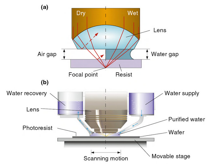
[9/16] Immersion Lithography
I feel obliged to briefly explain another feat of engineering that will play into my final points at the end of this thread. The latest logic and memory chips heavily rely on a new type of scanner technology called immersion lithography. In short, the air gap between the lens and the wafer is replaced with water. By doing this the virtual size of the lens is increased, and better resolution can be obtained.
At the time this was being developed by ASML, many folks in litho world thought this was crazy, and every PowerPoint presentation on the topic had images of surfboards and killer waves. If you look back at my list of ASML’s scanners, you will see a series of prototypes and then the beta tool (1700i) before the final production tool was realized.
This could be considered another modern marvel in that the water film has to be suspended as the lens scans on and off the wafer. There can't be a single bubble in this moving water film. There can’t be a single droplet left on the wafer, or it leaves a mark in the pattern. All this has to happen as these stages are moving around at tremendous speeds.
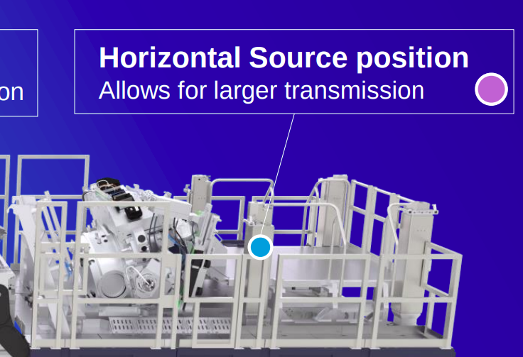
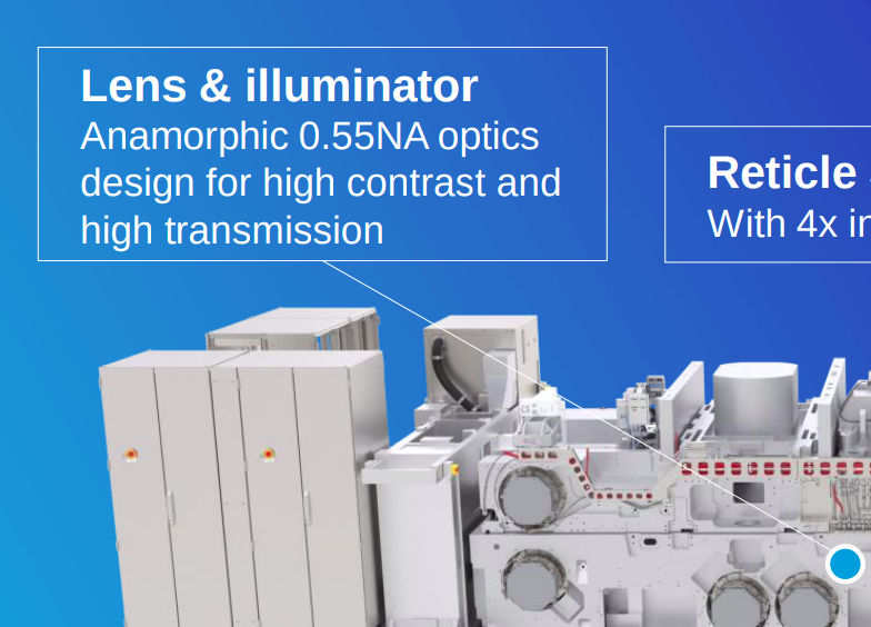
[10/16] The EUV Era
We’ve discussed the DUV platforms and what ASML was working on for 35 years to improve their commercial viability. But as we jump into the two EUV platforms, we have a new set of engineering challenges that make that development work seem simple.
Whereas the DUV platforms could rely on a common set of fundamentals to be borrowed for each new source and lens type that improved the resolution, EUV systems operate in a completely different way—essentially, ASML had to reinvent every subcomponent, not just the platform itself.
I summarize the 5 major differences between all the prior DUV systems and the new EUV tools here. Each of these required decades of R&D and incremental improvements before something that would be even close to production-worthy could be realized.

[11/16] The EUV Development Timeline
EUV lithography is the most complex and ambitious undertaking in lithography to date. It's arguably the most complex machine ever made on a commercial scale. The development for it started back in the mid-1980s and continues to this day. ASML didn’t do this alone; they benefited greatly from decades of work by more than 30 different organizations across the globe.
EUV lithography is the most complex and ambitious undertaking in lithography to date. It's arguably the most complex machine ever made on a commercial scale. The development for it started back in the mid-1980s and continues to this day. ASML didn’t do this alone; they benefited greatly from decades of work by more than 30 different organizations across the globe.

[12/16] Exposing Product Wafers Drives Learning
Let’s revisit our list of ASML’s scanner models again; refer to Column C for the tool types. As you can see, the vast majority of these tool models were HVM machines running product wafers in the fabs that today can cost as much as $20,000 each.
Prototype tools are the first systems where basic R&D on new subcomponents can be developed. For the most part, these were the early immersion and EUV systems where a big upending for how the process operated was needed. Beta tools are precursors to the HVM tools, but they are not commercially viable yet to the point where a fab can get sufficient ROI on the machine. But with these beta systems, fully integrated test lots can be run to get electrical data and, more importantly, a significant amount of overlay data on the machine to prepare it for HVM.
Then we have the HVM systems, which is where the real magic happens; money is made by the fab. As ASML progressed through each iteration of ROI improvement, millions of wafers had to be run on each tool model to enable this. Vast amounts of data are collected on real products and evaluated to understand what adjustments can be made for the next model to improve both the overlay and throughput.
Therefore, this learning process doesn’t happen in a vacuum back at the ASML factory; the fabs need to invest billions of dollars running millions of wafers. Only in this way can ASML inch forward and squeeze out fractions of a nanometer of improvements in the overlay performance while maintaining or improving the speed. This is what really sets lithography apart from the other unit processes.

[13/16] Lithography is Winner Take All.
The graveyard of scanner companies is full. One might think this is due to how other companies fail in their line of business—a botched product launch, missed timelines, economies of scale. Here again lithography is a different beast. The reason is hardware matching; in short, there is a yield and ROI benefit to only running one type of scanner vendor and their matching stages.
The extreme degree of precision for overlay is reaching the sub-nanometer scale. At these levels, each wafer chuck has a visibly different overlay signature. Indeed, a common way to gauge scanner overlay is what’s called Single Machine Overlay, or SMO. In this test a wafer is exposed on one chuck on one scanner, then the pattern is etched. Then the wafer is exposed on the exact same chuck and scanner to see the ultimate overlay performance of the machine. The hardware signature is removed in this way.
But fabs can’t operate that way for logistical reasons. So the realistic measurement is Match Machine Overlay. In this method a set of scanners is matched to each other with a correction algorithm that tries to wash out the different hardware signatures. Now think about what happens if two different scanner vendors are used. There is an overlay penalty and ultimately a yield and ROI penalty to that.
In fact, Nikon’s immersion scanners are just as good as ASML’s. Fabs would love to introduce a fleet of Nikons into their fabs to compete with ASML just to put price pressure on both vendors. The last thing a fab wants is a vendor monopoly. But unfortunately that’s not how the physics works. This is the reason Nikon is losing market share to ASML every year. It’s winner take all.

[14/16] The Chip War
Advanced lithography tools are at the heart of the chip war. Indeed, the first salvo fired over the bow was the banning of ASML’s EUV scanners from export to China. This was followed by 2 export actions blocking the most advanced DUV immersion systems made by both ASML and Nikon.
The response was expected and immediate. A handful of Chinese SMEs would enter into the scanner building business to make tools that would replace the banned systems. We’ve seen a lot of speculation about how long this would take to do.
Most of the arguments I’ve seen revolve around China’s great success in other industries, electric vehicles, aerospace, etc. All very impressive and accomplished under very tight timelines. But the development of those machines has an entirely different set of input factors that affect the timeline. Each are very different.
I don’t think that fast progress in one area automatically equates to success in another. I also don’t think it’s just a given that the development of lithography systems can just be leapfrogged into the most advanced tool ever made by mankind. I think a learning process has to happen very similar to the way ASML did it. And as you can see from my tool model list, this took about 50 iterations in an HVM capacity, with the prototype R&D happening in parallel.

[15/16] So how long then?
2035
NXT:2000i equivalent specs
2045
NXE:3800E equivalent specs
- Look at this list and tell me it won’t take at least 20 iterations and a fleet of new models being installed every year?
- How many wafers need to be run on each new model?
- How do you get around the hardware matching dilemma with most of these fabs already running a full fleet of ASML scanners?
- What fab is going to eat the yield losses?
- How do you compete with ASML and Nikon, who both have proven ROI on commercially viable machines? (Not all immersion scanners are blocked)
So many questions.
- The “science” part is a given; obviously that EUV development timeline that took ASML 3 decades needs to be compressed into a fraction of that.
- The “engineering the sh/t out of it” part is so obvious it’s irrelevant.

[16/16] Overlay = 3 meters
[end]
[end]
• • •
Missing some Tweet in this thread? You can try to
force a refresh