Semiconductors - Follow me to learn all about microchips & how we print them. My web scraper is a live dashboard for the freshest tech news & press releases.
Oct 18 • 16 tweets • 13 min read
[1/16] 🧵 A History of ASML’s Scanners
Enabling the AI Revolution with chip printers—the most complex machines ever built.
[2/16] The List
Here we have my list of all the ASML’s scanner models installed over the past 35 years. It’s not an exhaustive list; I’m sure I’ve missed a few, but it’s what I was able to put together based on the tools I’ve run (which is most of them) or models my friends have told me they’ve used. As you can see by the super small font I had to use here, it’s a big list of around 50 different tool models. Let’s do a deeper dive on this history in this thread and how we got to the latest EUV tools being installed today in the most advanced chip factories around the world.
đź§µ I was traveling this week, and I didn't have a chance to do a thread on ASML's Investor Day. In my opinion, this is one of the most impressive yearly updates given by any company, and they make all of the presentations public. It combines deep insight into the overall market, their finances, and the complex technical roadmap for their tools. @BeuvingJordy already did a thread on the financials, so I'll focus on the technical aspects in this thread.
One of the more important slides in their EUV talk discusses the history and roadmap for the source power. Unlike prior generations of projection lithography, EUV consumes huge amounts of energy to generate the source photons, yet only 2% of this ever reaches the wafer. For this reason, this is the top metric that determines how many tools a fab needs to purchase and what the ROI will be on that fleet. Another important thing to understand is that as the chip geometry is scalled down, the required dose to pattern a chip goes up exponentially. So the timing for which the source power increases has many consequences.
Look at the source power plot to the left. You'll see that the first decade saw very few increases in power. Then it jumps to 200W in 2018, the year EUV was introduced into production. This was the magic number. It was the point at which EUV became cheaper than 4 passes of multipatterning with immersion tools; hence the reason it was introduced at the 7nm node.
This year ASML began shipping their 500W sources, and they swap this for the installed tools in the field as an upgrade. You see in the graphic one of the main methods they get higher source power is increasing the rate of the tin droplets. These droplets are hit with a high-power CO2 exicmer laser to strike a plasma; the light emitted from the plasma is the EUV light used to image the chip.
The 200W source vaporized about 50000 droplets per second. I don't have my notes on their SPIE talk for this in front of me, but presumably the new 500W source is running closer to 100000 droplets per second, and this would need to double to get to 1000W by 2030. In fact, the laser strikes each droplet twice: one pulse to flatten it into a pancake and a second main pulse to strike the plasma. I remember from their SPIE talk that ASML is trying to get rid of the pre-pulse in order to get the droplet rate up.
Jan 24, 2024 • 7 tweets • 5 min read
đź§µHigh-NA EUV Design - EXE:5000
ASML shared this in their earnings report today, and here are a few observations.
"Common technology with NXE": This has always been one of ASML's secrets to success. Lithography machines are very complex systems, and before ASML came along, these tools were not designed to have modular components, at least not the main ones like the stages or lens. They also weren't designed with a vision of what future tools would look like. By sharing modular components between the different generations of tools, this streamlines the development process and ultimately the cost of producing them.
It also allows for outsourcing the supply of the big components, so ASML can focus on the assembly and service pieces. Each supplier thus focuses on the quality and technology associated with their module. Compare that to how other complex machines are made, such as the Boeing 787. Would they be better served to outsource the big components, such as the wings or cockpit, and just focus on assembly?
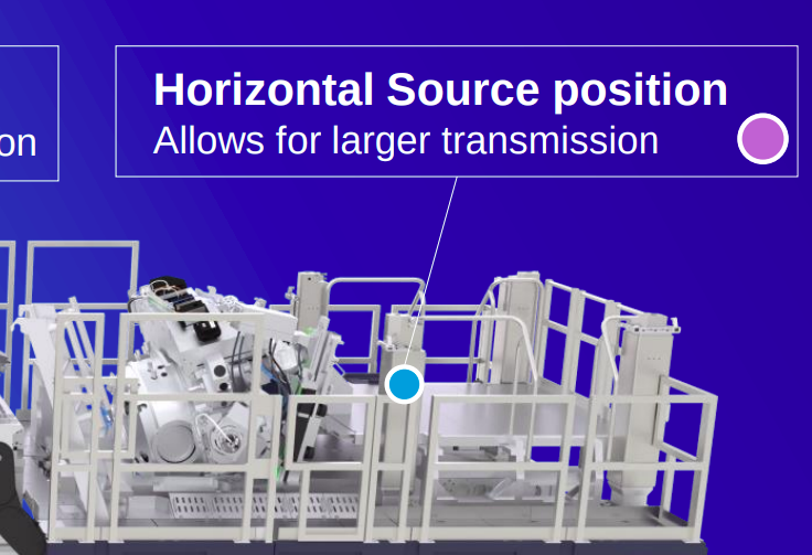
Horizontal Source Position.
This may seem trivial, but it's a brilliant design change. The prior NXE system had the source aiming at an upward angle into the lens, and it sat half-way below the floor. So right off the bat, by moving this up, it allows for access to every side of the source. IMO, this is an important move because maintaining the source is a huge deal for making it reliable in a production environment. It also makes it easier to upgrade and make changes in the field. This will be important if ASML intends to make good on its source roadmap.
They're saying here that repositioning it improves transmission. I can only assume that changing the angle at which it hits the lens ultimately allowed for the removal of one of the lens mirrors. Why is that important for transmission? Because the multi-layer lens mirrors have very poor reflectance, each pass off a mirror loses 30% of the photons. So by removing a mirror, you gain 30% productivity. That's a huge win.