Etching is a process used to remove material from the wafer surface to meet the design requirements of an integrated circuit (IC).
There are two types of etching: one is patterning etching, which removes material in specified areas, such as transferring patterns from a photoresist or hard mask layer onto the substrate film. Another type is blanket etching, which removes the entire surface film to meet process requirements, for example, backside wafer etching. (1/11) 🧵
There are two types of etching: one is patterning etching, which removes material in specified areas, such as transferring patterns from a photoresist or hard mask layer onto the substrate film. Another type is blanket etching, which removes the entire surface film to meet process requirements, for example, backside wafer etching. (1/11) 🧵
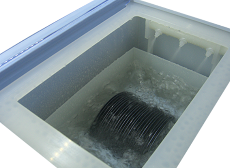
Etching also can be categorized into two types based on characteristics: wet etching and dry etching. Wet etching is typically performed at room temperature, requiring no additional vacuum equipment, RF systems, or gas delivery setup. The process is relatively easy to control, making the equipment significantly cheaper than that used for dry etching. Below, we will introduce each in detail. (2/11)
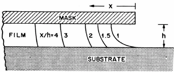
However, the chemical reaction itself has no directional preference—making wet etching inherently isotropic.
Isotropic etching means that material is removed not only vertically but also laterally, leading to an undercut effect. This undercut prevents accurate pattern transfer to the wafer and can cause line collapse in sub-3-micron processes, leading to their gradual replacement by dry (plasma) etching. (3/11)
Isotropic etching means that material is removed not only vertically but also laterally, leading to an undercut effect. This undercut prevents accurate pattern transfer to the wafer and can cause line collapse in sub-3-micron processes, leading to their gradual replacement by dry (plasma) etching. (3/11)
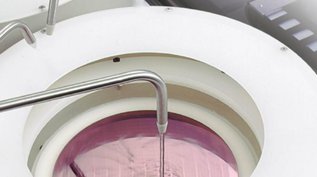
Common wet etching processes are applied to silicon dioxide (SiO₂), single-crystal silicon, polysilicon, silicon nitride (Si₃N₄), and various metals.
⚆ Silicon dioxide etching typically uses hydrofluoric acid (HF) diluted at 6:1 or 10:1, since a 1:1 HF mixture etches too rapidly at room temperature, making it difficult to control the rate and uniformity. A 10:1 HF solution can also be used to remove the native oxide layer on the surface of a silicon wafer.
⚆ Single-crystal silicon etching is used to form isolation regions between transistors, while polycrystalline silicon etching is used to form gate electrodes and local interconnects. It’s typically performed using a mixed solution of nitric acid (HNO₃) and HF. In this process, nitric acid oxidizes silicon into silicon dioxide, which then reacts with HF and dissolves, exposing the underlying silicon to further oxidation by nitric acid. Through repeated cycles of these reactions, silicon is gradually etched away.
⚆ Silicon nitride etching is commonly used in insulation processes. Phosphoric acid (H₃PO₄) is the typical etchant because its reaction products, silicon phosphate (Si₃(PO₄) ₄) and ammonia (NH₃)—are both soluble in water.
⚆ In metal etching, a mixture of phosphoric acid, acetic acid, and nitric acid was traditionally used for aluminum patterning processes. However, as advanced process requirements have evolved, it is now mostly used to evaluate the quality of PVD-deposited aluminum films. (4/11)
Interestingly, semiconductor engineers once sought to eliminate all wet processes from chip manufacturing, but the widespread adoption of CMP and CVD has made it difficult to completely remove wet processing. Because wet processes offer high selectivity, etching efficiency can also be used to evaluate film quality, making this another important application of wet process equipment. (5/11)
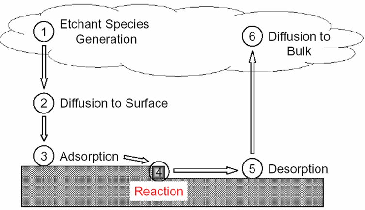
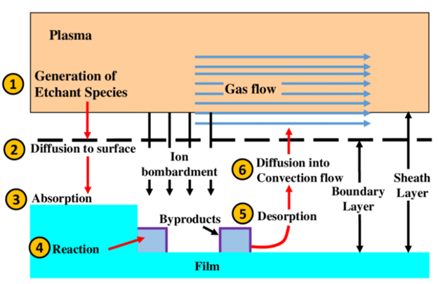
Dry etching uses gaseous chemical etchants to react with materials and produce volatile byproducts that can be removed from the substrate. At the same time, plasma bombardment of the wafer surface causes ion impacts that not only physically remove surface material but also break the chemical bonds of surface atoms, significantly increasing etching efficiency. (6/11)
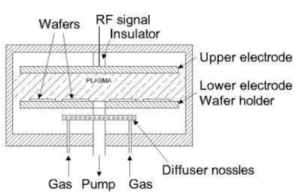
Process:
⚆The etching gas is first introduced into a vacuum reaction chamber
⚆After pressure stabilization, an RF discharge generates plasma
⚆Some etchant molecules are decomposed by high-energy electron collisions, producing reactive free radicals.
⚆These radicals diffuse through the boundary layer to the wafer surface and are adsorbed
⚆Under ion bombardment, the radicals quickly react with surface atoms to form gaseous byproducts, which detach from the wafer surface, diffuse back through the boundary layer, and are eventually exhausted from the chamber. (7/11)
Next, we will introduce process control in etching:
⚆ Etch rate, which measures how quickly material is removed during etching. It is calculated as: Etch Rate = (Initial Thickness−Final Thickness)/ Etching Time
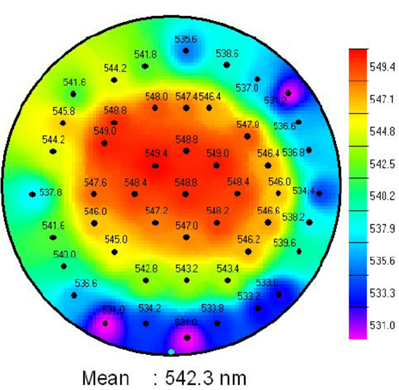
⚆ Uniformity is a key parameter to ensure consistent etch rates and high repeatability across the entire wafer. It is determined by measuring the etch rates at multiple predefined points on the wafer and calculating their variation.
⚆ Etch selectivity refers to the ratio and difference in etch rates among the photoresist, films, and substrate during the etching process. Selectivity = Etch Rate1/Etch Rate2 (8/11)
⚆ Etch rate, which measures how quickly material is removed during etching. It is calculated as: Etch Rate = (Initial Thickness−Final Thickness)/ Etching Time
⚆ Uniformity is a key parameter to ensure consistent etch rates and high repeatability across the entire wafer. It is determined by measuring the etch rates at multiple predefined points on the wafer and calculating their variation.
⚆ Etch selectivity refers to the ratio and difference in etch rates among the photoresist, films, and substrate during the etching process. Selectivity = Etch Rate1/Etch Rate2 (8/11)
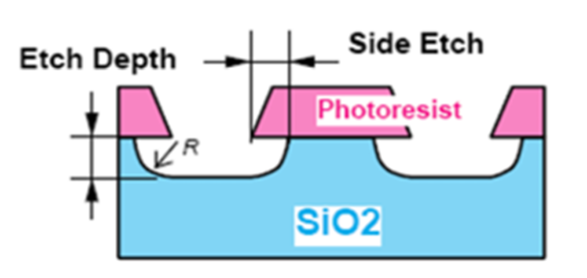
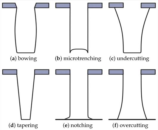
⚆Etch profile/outline is one of the most critical characteristics, as it directly affects subsequent deposition processes. The shape of the profile varies depending on the process, but the ideal form is vertical, since it ensures that the pattern defined in the photoresist is fully transferred without critical dimension (CD) loss.
⚆Over-etching occurs because etch rates and film thicknesses vary across the wafer, often leaving some areas where the film has not been completely removed. The additional etching step used to eliminate these remaining films is called over-etching.
⚆Residue refers to unwanted material that may remain on the sidewalls or wafer surface after etching. Such residue often results from incomplete over-etching caused by the wafer’s complex surface topology.(9/11)
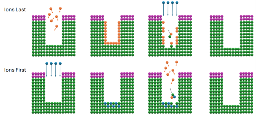
Another worth mentioned topic is Atomic Layer Etching (ALE) refers to a process that removes material with atomic-level precision, typically at an average rate of about 0.1 nm/min.
There are two types of ALE processes — ions-first and ions-last — depending on whether ions are introduced in the first or last step.
Ions-last: Plasma such as Cl₂, O₂, or CHF₃ (depending on the substrate) is introduced into the reaction chamber first. The plasma reacts with the surface, forming bonds with the layer in a process called adsorption. Like ALD, this reaction is self-limiting, stopping once the entire surface is occupied. Next, Nitrogen or Argon are used to purge unreacted species. Finally, ions (e.g., Ar⁺) bombard the surface to remove the reacted layer in a step known as desorption.
Ions-first: Ions are introduced first and implanted into the surface through diffusion or heating. Plasma is then introduced to remove the modified surface layers.(10/11)
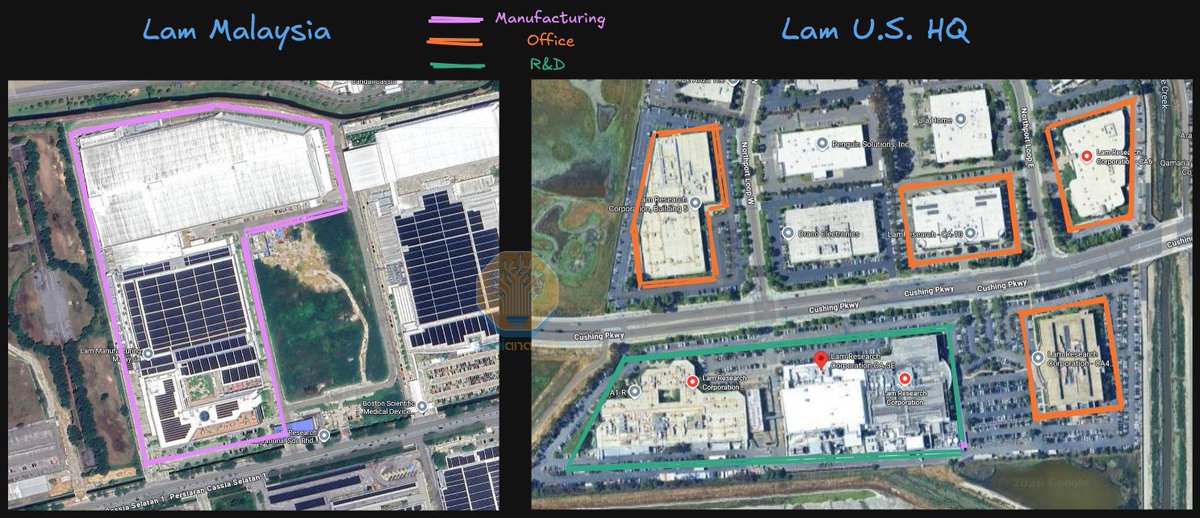
In the etch equipment market, Lam holds the leading position, followed by TEL and AMAT. As mentioned earlier, wet process tools are relatively simple, and with rising cleanliness requirements across advanced nodes, several Taiwanese companies—GPTC, Scientech, SHT and GPM—have entered the competition. (11/11)
• • •
Missing some Tweet in this thread? You can try to
force a refresh