 While it is true that Kimi K3 uses Kimi Delta Linear Attention (KDA) in 3 out of every 4 layers and that KDA reduces KV-cache transfer bandwidth by up to 10x compared with comparable full global-attention models, the important missing piece is that Kimi K3 requires WideEP to serve. 2/8🧵
 As we continue to monitor the status of datacenter delays, whether they are real, whether they are fake... some are out and out delayed because of -> building gas pipelines and receiving permits for power generation equipment. (2/8)
 Kimi K3 is actually quite positive for NVIDIA, as large-model inference is where the NVL72 shines. Because K3 has more than 2.8 trillion parameters, it requires a large scale-up domain to store its weights. 2/8🧵
 Before the first strike ever came down on Tehran, OSINT accounts right here on this platform were tracking the military buildup in the Middle East in near real time.
 TSMC’s Open Innovation Platform has turned Synopsys, Cadence, Arm, Rambus, Alphawave, and dozens of IP vendors into a pre-validated tape-out network. And that moat is measurable. (2/8)
 Scale-across has been widely popularized by Nvidia last year, but is now often used imprecisely as a generic term to talk almost about any Datacenter interconnect network. To make it short, scale-across refers to backend datacenter interconnect networks that are used to connect multiple datacenters all together to form a single, coherent cluster. (2/7)
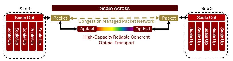
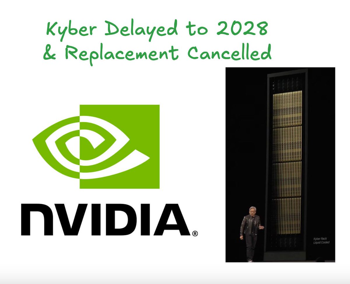 Kyber NVL144 rack architecture has been delayed to 2028 as the PCB midplane remains challenging from a manufacturability standpoint. NVL576, which connects 8x Oberon racks over CPO between the NVSwitches, is also likely delayed or restricted to small volumes given the current challenges with CPO. 2/6🧵
 It is first helpful to understand how the underlying models work. Opus, GPT 5.5, etc (the models) are all stateless -- they remember nothing between requests. That is, each time you press "enter" at the prompt factory, the harness rebuilds the entire conversation and ships it (this is why prompt caching is so important!). There is no memory sitting on the server. Whatever the model "knows" about your session exists only because the harness packed it into that one request. (2/5)
 The idea is simple: maintain HBM4 performance while drastically reducing the reliance on expensive, supply-constrained advanced packaging.
 So why EMIB?
 This all comes against the backdrop of NVIDIA’s market share being eroded by Trainium, TPUs, and AMD chips. For NVIDIA to maintain pole position, it must be aggressive in execution. Manufacturing execution issues like this will only lead to more market share being chipped away. 2/4🧵
 Tungsten is a great example.
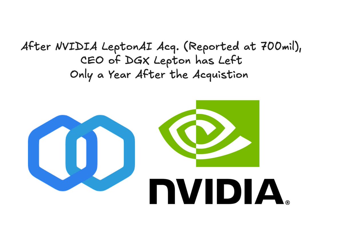 Initially, NVIDIA claimed that Lepton’s core software platform would be open-sourced by 2026. That has yet to happen. While we were skeptical, we wanted to believe that NVIDIA would open-source the core Lepton software platform, given that Lepton’s CEO is the co-creator of Caffe, ONNX, and PyTorch. 2/7🧵
 The substitution math is the part to internalize. Tasks that used to need a junior analyst for several hours, converting a model to a dashboard, building chart packs from earnings, rebuilding a comp set, now resolve in minutes for a few dollars of tokens. The blended Opus 4.7 cost we observe is about $0.99 per million against $5/$25 sticker, mostly because agentic workloads run 300:1 input-to-output ratios and cache hit rates above 90% pull the effective price down. Thats a real change in the unit economics of professional services, not a 10% efficiency gain. (2/4)
 The important signal is that this is likely a spot price index not term pricing. Our neocloud survey for 1-year H100 contract prices have isntead climbed from a trough of roughly $1.70 per hour late last year to about $2.65 per hour today. (2/5)
 AI demand has surged so high that import prices for computers and semiconductors rose 3.6% in May, now up 14.4% year-to-year. This is so far from anything in the historical record that 'fastest ever' doesn't do justice to it. (2/4)
 Israel is the perfect case study to understand what’s really going on: high car ownership, zero domestic production & no restrictions on auto imports from China. Here’s what the data shows:
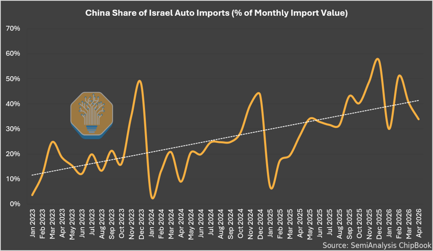
 Recently, we purchased one of each Anthropic/OpenAI subscription plan and randomly ran long horizon coding tasks until we exhausted the weekly limit. It's widely believed that a $200/month plan maxes out at ~$2000/month worth of tokens (assuming API pricing). However, we found that the subscriptions are actually far more generous. (2/4)
 Let’s focus on the first for now; Assembly.
 Here is what the supply chain looks like:
 The site has two key sections: Section A and Section B.