Everyone's always talking about agentic coding harnesses: Claude Code, Codex, OpenCode, Pi... the list goes on. But what's the difference between all of them? What even Is a harness anyway?
In this thread, we'll take a look under the hood. (1/5)🧵
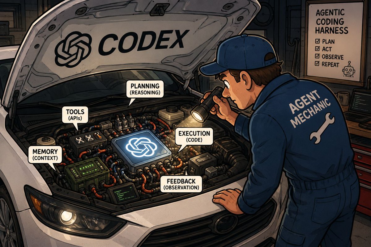
It is first helpful to understand how the underlying models work. Opus, GPT 5.5, etc (the models) are all stateless -- they remember nothing between requests. That is, each time you press "enter" at the prompt factory, the harness rebuilds the entire conversation and ships it (this is why prompt caching is so important!). There is no memory sitting on the server. Whatever the model "knows" about your session exists only because the harness packed it into that one request. (2/5)
So a "harness" is really a context orchestration tool. Every request body it builds typically has the same three parts:
🟠 System Prompt: the "you are Claude Code" setup, plus injected stuff like your file tree or recent commits
🟠 Tool Definitions: a list of JSON schemas describing available tools the model has to "act", I.e., Bash, FileRead, etc.
🟠 Messages: the chronological list of user/assistant messages, as well as thinking blocks.
Since the model is stateless, the harness reassembles and resends all of these parts every turn. What differs between Claude Code, Codex, and OpenCode is not only the TUI/UX features, but how this context is managed. For instance, people like Pi because you have more control over how the harness is managed and therefore how the context is. (3/5)
When you send a message, the harness will route your request to the appropriate LLM server, then apply some chat templates to convert the HTTP request to something the model can better understand. The harness will also add more advanced parameters to control cache, max output tokens, and other things depending on the type of request.
Given the context described above, the model will decide what tools, if any, to use. If the model chooses a tool, it will literally generate the appropriate tool use JSON and return it in the response body! This tool use is then parsed in the harness on the host machine and executed, and its output is automatically sent back to the LLM for processing. (4/5)
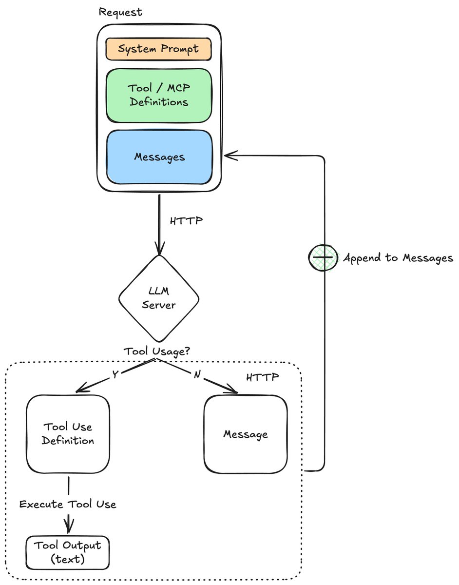
So while all harnesses make slightly different decisions while performing this "plan, act, verify" pattern, this loop is the common skeleton driving all agentic tasks. So let's stop talking about harnesses like they're magic! While good harness engineering helps, the real power is still in the models themselves. Everything else is just REST all the way down. (5/5)
• • •
Missing some Tweet in this thread? You can try to
force a refresh

MASSIVE DELAY: Just 3 months after Jensen demoed Kyber NVL144 at GTC, it has faced major setbacks and has been delayed by more than 12 months, pushing it back to 2028. Below, we explain why Kyber has faced massive delays and why NVIDIA’s NVL72x2 back-to-back rack architecture was also cancelled, leaving Rubin Ultra with a limited scale-up domain. 👇️ 1/6🧵
Kyber NVL144 rack architecture has been delayed to 2028 as the PCB midplane remains challenging from a manufacturability standpoint. NVL576, which connects 8x Oberon racks over CPO between the NVSwitches, is also likely delayed or restricted to small volumes given the current challenges with CPO. 2/6🧵
NVL72x2 back-to-back rack architecture was the new proposed architecture NVIDIA was developing as an alternative to Kyber. It was designed to increase the pure-copper NVLink scale-up world size by placing two Oberon racks back-to-back. However, it has since been cancelled due to heavy pushback from CSPs and hyperscalers over its odd design and heavy operational burden. 3/6🧵
This last week JEDEC announced a new standard for SPHBM4: Standard Package High Bandwidth Memory (JESD330-4).
It utilizes the same DRAM stacks as HBM4, but swaps in a different buffer die. The goal? Enable HBM assembly in standard packaging and break the AI Advanced Packaging bottleneck. (1/6)🧵
The idea is simple: maintain HBM4 performance while drastically reducing the reliance on expensive, supply-constrained advanced packaging.
How? By slashing the pin count to 1/5th but quadrupling signal speeds to 32 Gbps. This allows HBM-level bandwidth using standard substrates, while pushing the connection distance out to 20mm for vastly superior thermal management.
Here is why SPHBM4 is a massive win for the substrate industry: (2/6)
🟠 It blows up the physical size of the substrate.
Traditional HBM must sit microscopic millimeters away from the GPU because wide parallel signals degrade instantly over distance.
Because SPHBM4 uses high-speed serial lanes, memory can sit up to 20mm away. This extra breathing room means there is room for more HBM per package, as chip packaging footprints get much larger, dramatically driving up the total square footage of substrate material needed per chip. (3/6)
Google's next TPU, codenamed Humufish, is set to use Intel's EMIB-T instead of TSMC CoWoS.
Nearly every leading AI training accelerator today is packaged on a TSMC 2.5D flow, and almost all of it is CoWoS. CoWoS is the industry default, which is exactly why a flagship part moving off it is worth attention.
The core difference. CoWoS places all dies on a single large silicon/RDL interposer. EMIB embeds small silicon bridges directly in the organic substrate, only where die-to-die links are needed. (1/4)🧵
So why EMIB?
🟠 EMIB isn't bound by the interposer reticle limit. A CoWoS silicon interposer is printed by lithography, so it is capped by the reticle limit; the monolithic version (CoWoS-S) maxed near 3.3x, which is why TSMC moved to CoWoS-L. EMIB is not bound by the reticle limit, so it’s a much more scalable technology.
🟠 Efficiency and cost. EMIB packaging is meaningfully cheaper, since it drops the costly interposer entirely. EMIB also uses silicon far more efficiently than CoWoS. A wafer is round, so large interposers waste area at the edge and yield worse as they grow, while tiny bridges tile densely with little waste. It also gives buyers a second source outside TSMC. (2/4)
Humufish is using EMIB-T. The "T" is TSV. Plain EMIB has no vias in the bridge, so power has to detour around it through the substrate, which strains power delivery. EMIB-T sends power vertically straight through the bridge, with added capacitors and a ground plane for cleaner power. That is what makes it ready for next-gen HBM and higher-bandwidth interconnects. (3/4)
INTERESTING: Only 3 months after Rubin Ultra was announced at GTC 2026, the original 4-die Rubin Ultra has been cancelled due to manufacturing execution concerns. The new “Rubin Ultra” is half the size/~ half the real-world performance of the original Rubin Ultra. 1/4🧵
This all comes against the backdrop of NVIDIA’s market share being eroded by Trainium, TPUs, and AMD chips. For NVIDIA to maintain pole position, it must be aggressive in execution. Manufacturing execution issues like this will only lead to more market share being chipped away. 2/4🧵
A good chunk of inference for the most successful AI agent, Claude Code, is done on Trainium, while Claude training is done on TPUs. Just a year ago, it would have been unimaginable that TPUs and Trainium could grow this rapidly, while the CUDA moat slowly eroded. 3/4🧵
One of the most underappreciated ways to play the AI semiconductor buildout may be through materials rather than chips themselves.
As the industry races to produce more advanced semiconductors, demand isn’t just rising for GPUs and wafer fab equipment, it’s rising for the critical materials that make modern chips possible. (1/6)🧵
Tungsten is a great example.
It is one of the most critical materials in semiconductor fabrication, prized for its high-temperature stability and resistance to electrical wear. Fabs rely on CVD to fill the deep, high-aspect-ratio vertical vias that link multi-layered chip architectures, while utilizing PVD to deposit the ultra-thin structural barrier layers surrounding them. Because it spans both core deposition categories, tungsten is completely non-negotiable for advanced chip production. (2/6)
What’s interesting is that supply appears increasingly constrained. High-purity tungsten metal powder is the primary raw material used to manufacture WF₆ (tungsten hexafluoride, the gas used in CVD). The raw supply chain is overwhelmingly dominated by China, which controls roughly 80% of global tungsten mining, refining, and powder processing capacity.
China exports YTD are down ~50% YoY, and the data demonstrates the pricing pressure global customers are facing on this critical component. (3/6)
BREAKING NEWS: The Founder/CEO of LeptonAI has left only a year after LeptonAI’s acquisition. This is quite shocking, as Jensen reportedly spent $700M acquiring LeptonAI. What did he see? DGX Lepton flopped and got nowhere near the success Jensen expected. 1/7🧵
Initially, NVIDIA claimed that Lepton’s core software platform would be open-sourced by 2026. That has yet to happen. While we were skeptical, we wanted to believe that NVIDIA would open-source the core Lepton software platform, given that Lepton’s CEO is the co-creator of Caffe, ONNX, and PyTorch. 2/7🧵
One speculation for why Lepton’s CEO left is that Jensen ultimately changed his mind and did not approve open-sourcing Lepton. In acquisitions, standard practice is for vesting to happen over multiple years. 3/7🧵