ASML is the most important company you've never heard of.
The $300B+ Dutch firm makes the machines that make semiconductors. Each one costs $150m and access to them are a huge geopolitical flashpoint.
Here's a breakdown 🧵
The $300B+ Dutch firm makes the machines that make semiconductors. Each one costs $150m and access to them are a huge geopolitical flashpoint.
Here's a breakdown 🧵
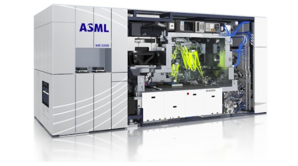
1/ What *exactly* does ASML sell?
Its key product is an extreme ultraviolet lithography (EUV) machine, which uses advanced light technology to "print" tiny circuits onto Silicon wafers.
Only ~50 are made a year and ASML has a near monopoly on the machine technology.
Its key product is an extreme ultraviolet lithography (EUV) machine, which uses advanced light technology to "print" tiny circuits onto Silicon wafers.
Only ~50 are made a year and ASML has a near monopoly on the machine technology.
2/ You def know ASML's main clients: Intel, Samsung and Taiwan Semiconductor Manufacturing Co. (TSMC).
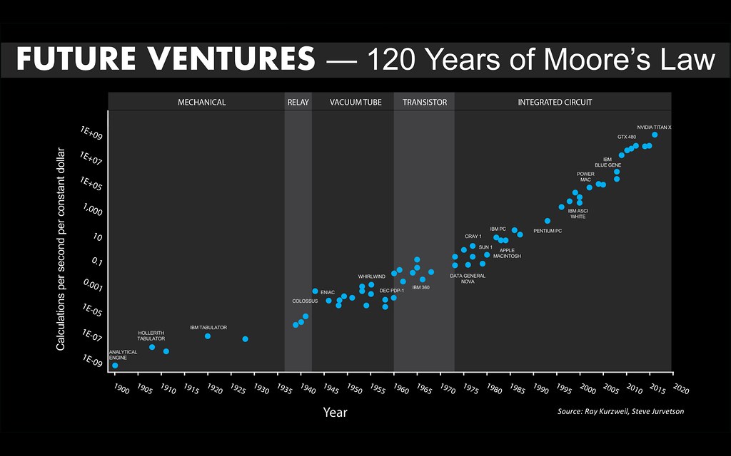
They need EUV to keep Moore's Law ("# of transistors on microchips doubles every 2 years") alive and continue to advance computing.
Total ASML sales in 2020 = $16B+.
They need EUV to keep Moore's Law ("# of transistors on microchips doubles every 2 years") alive and continue to advance computing.
Total ASML sales in 2020 = $16B+.
3/ The ASML story begins in 1984, as a joint venture between Dutch conglomerate Philips and an electronics maker called Advanced Semiconductor Materials Int.
The project had a very humble start: it was launched in a shed behind a Philip's building in Eindhoven, Netherlands.
The project had a very humble start: it was launched in a shed behind a Philip's building in Eindhoven, Netherlands.
4/ The venture's first product was called the PA 2000 stepper (think a slide projector "projecting" designs on silicon).
For years, the product failed to make headway against leading Japanese competitors (Nikon, Canon) and, in 1990, ASML was spun out as its own company.


For years, the product failed to make headway against leading Japanese competitors (Nikon, Canon) and, in 1990, ASML was spun out as its own company.


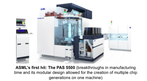
5/ ASML scored its 1st hit product in 1991, giving it momentum to IPO in 1995.
Soon after, it acquired a # of US lithography firms and -- by the end of 1990s -- it had comparable market share to Nikon and Canon.
From there, ASML made 2 big bets that separated it from the pack.
Soon after, it acquired a # of US lithography firms and -- by the end of 1990s -- it had comparable market share to Nikon and Canon.
From there, ASML made 2 big bets that separated it from the pack.
6/ Both bets were made to keep up with Moore's law.
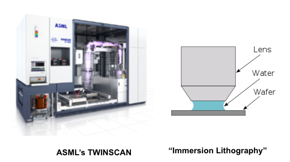
First: In 2006, ASML released its TWINSCAN system using immersion lithography (it utilizes water as lens to shrink the laser's wavelength = more circuits on chip).
It was ASML's first market-leading product.
First: In 2006, ASML released its TWINSCAN system using immersion lithography (it utilizes water as lens to shrink the laser's wavelength = more circuits on chip).
It was ASML's first market-leading product.
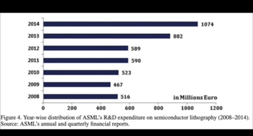
7/ Also in the mid-2000s, ASML started spending huge R&D on EUV technology.
It was a massive risk, though: EUV lithography would require Samsung, Intel and TMSC to completely rebuild and redesign their fabrication plants.
From 2008-14, ASML put $5B+ into EUV research.
It was a massive risk, though: EUV lithography would require Samsung, Intel and TMSC to completely rebuild and redesign their fabrication plants.
From 2008-14, ASML put $5B+ into EUV research.
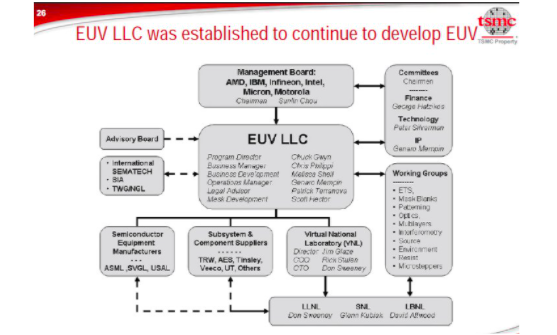
8/ The science behind EUV was established in the late 1980s. It was a US-led effort between the Dept. of Energy and industry (e.g. AMD, IBM, Intel).
ASML licensed EUV tech in 1999. Canon elected not to pursue it due to financial problems while Nikon chose to develop older tech.
ASML licensed EUV tech in 1999. Canon elected not to pursue it due to financial problems while Nikon chose to develop older tech.
9/ How EUV works today:
◻️ A tin droplet drops into a vacuum
◻️ It's pulsed by a high-power laser
◻️ Tin atoms are ionized, creating plasma
◻️ A mirror captures EUV radiation emitted by plasma
◻️ Mirror transfers EUV to wafer (wavelength=13.5 nanometers, basically X-ray level)
◻️ A tin droplet drops into a vacuum
◻️ It's pulsed by a high-power laser
◻️ Tin atoms are ionized, creating plasma
◻️ A mirror captures EUV radiation emitted by plasma
◻️ Mirror transfers EUV to wafer (wavelength=13.5 nanometers, basically X-ray level)
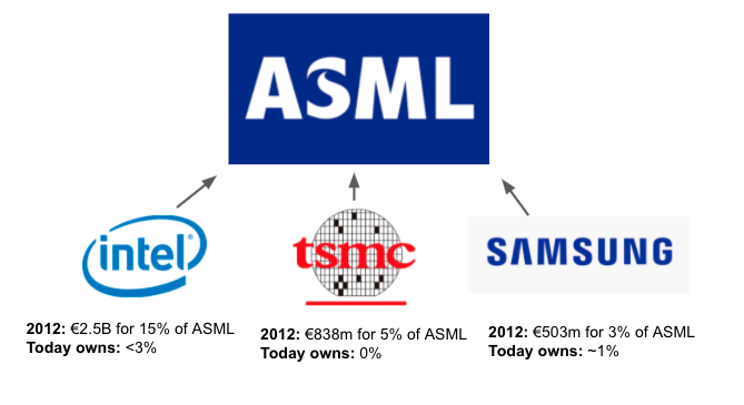
10/ The potential of EUV was so great that Intel, Samsung and TMSC -- all competitors -- jointly acquired 23% of ASML.
Intel put up the most: €2.5B for a 15% share (today, the firms have sold down most their stakes).
The first production-ready EUV machine was released in 2016.
Intel put up the most: €2.5B for a 15% share (today, the firms have sold down most their stakes).
The first production-ready EUV machine was released in 2016.
11/ Why are EUVs so expensive?
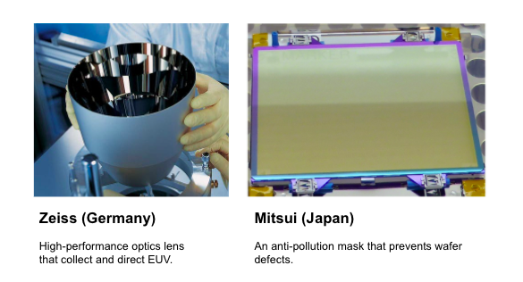
ASML plays a role similar to Boeing for airplanes (also $100m+ products): it's an integrator of 4750 global high-value parts suppliers:
◻️ Tooling equipment (US)
◻️ Chemicals (Japan)
◻️ Lens (Germany)
(Nikon/Cannon do most production in-house)
ASML plays a role similar to Boeing for airplanes (also $100m+ products): it's an integrator of 4750 global high-value parts suppliers:
◻️ Tooling equipment (US)
◻️ Chemicals (Japan)
◻️ Lens (Germany)
(Nikon/Cannon do most production in-house)
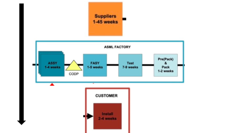
12/ Why can ASML only produce 50 EUV machines a year?
◻️ Co-ordinating 1000s of suppliers is very difficult (just like an aircraft)
◻️ Each machine is custom (30+ variables to choose from)
◻️ Lead-time are long (speciality parts like the Zeiss lens takes 40 weeks to produce)
◻️ Co-ordinating 1000s of suppliers is very difficult (just like an aircraft)
◻️ Each machine is custom (30+ variables to choose from)
◻️ Lead-time are long (speciality parts like the Zeiss lens takes 40 weeks to produce)
13/ The delivery process is nuts, too:
◻️ Each EUV weighs 180 tons
◻️ A disassembled EUV takes up 40 shipping containers
◻️ Shipping it (mostly to Asia) takes 20 trucks and 3 Boeing 747s
◻️ ASML teams must be on-the-ground to maintain them
◻️ The min spend to house EUVs is $1B
◻️ Each EUV weighs 180 tons
◻️ A disassembled EUV takes up 40 shipping containers
◻️ Shipping it (mostly to Asia) takes 20 trucks and 3 Boeing 747s
◻️ ASML teams must be on-the-ground to maintain them
◻️ The min spend to house EUVs is $1B
14/ Today, ASML has a 90% share in semi lithography (EUV and Deep UV).
EUV tailwinds are huge:
◻️ Semi CAPEX >$120B+ in 2021 (similar spend in following years)
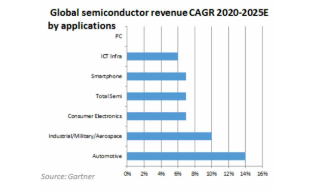
◻️ Key sectors (esp. auto AKA Tesla chips) will see growth for years
◻️ Transition to 5nm process requires more EUV
EUV tailwinds are huge:
◻️ Semi CAPEX >$120B+ in 2021 (similar spend in following years)
◻️ Key sectors (esp. auto AKA Tesla chips) will see growth for years
◻️ Transition to 5nm process requires more EUV
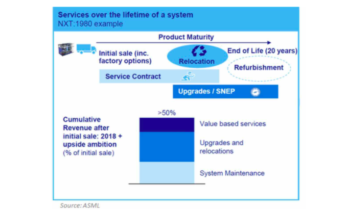
15/ Even if machine sales slow, ASML's business is increasingly shifting to system maintenance, relocation and upgrades.
Over a 20yr lifespan of an ASML machine, services-based sales may reach 50% of the initial machine price (w/ high margins)...across a growing installed base.
Over a 20yr lifespan of an ASML machine, services-based sales may reach 50% of the initial machine price (w/ high margins)...across a growing installed base.
16/ With chips needed in everything (data centres, AI, autos, mining), semis are the OIL of the 21st century.
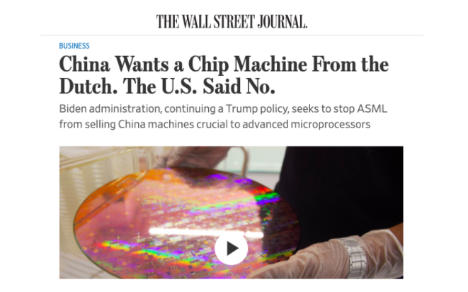
The US has even blocked Dutch exports of EUV-licensed tech to China. As the Tech Cold War heats up, expect to hear more of ASML: the $300B+ giant that started in a shed.
The US has even blocked Dutch exports of EUV-licensed tech to China. As the Tech Cold War heats up, expect to hear more of ASML: the $300B+ giant that started in a shed.
17/ If you enjoyed that, I write threads breaking down tech and business 1-2x a week.
Def follow @TrungTPhan to catch them in your feed.
Here's a related one that might tickle your fancy:
Def follow @TrungTPhan to catch them in your feed.
Here's a related one that might tickle your fancy:
https://twitter.com/trungtphan/status/1403004789642854409?lang=en
18/Sources
YouTube series from Asianometry is GREAT:
Pt 1.
Pt 2.
Seeking Alpha: seekingalpha.com/article/445004…
NY Times: nytimes.com/2021/07/04/tec…
YouTube series from Asianometry is GREAT:
Pt 1.
Pt 2.
Seeking Alpha: seekingalpha.com/article/445004…
NY Times: nytimes.com/2021/07/04/tec…
19/ Also discuss interesting topics like this once a week (with a healthy dose of dumb jokes) on the Not Investment Advice (NIA) podcast
Check here! linktr.ee/notinvestmenta…
Check here! linktr.ee/notinvestmenta…
20/ Here’s a cool vid showing the entire ASML EUV process. Pretty wild!
🔗
🔗
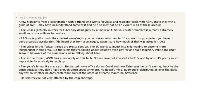
21/ This ASML thread made it onto Hacker News. The top comment adds a ton of great info:
news.ycombinator.com/item?id=282667…
news.ycombinator.com/item?id=282667…
• • •
Missing some Tweet in this thread? You can try to
force a refresh
