Castellanos Lab Profile picture
Research Professor working on 2D Mat at the Materials Science Institute of Madrid (ICMM-CSIC). My tweets shouldn't be considered as CSIC’s official position
Nov 4, 2023 9 tweets 5 min read
1/9 Sometimes you've projects you enjoy and you have a lot of fun. When they work... It's awesome!!!

Well, in the last year we've learnt how to make the thinnest possible ommelettes and we ended up using them to fabricate field-effect transistors 🤯


🧵👇 nature.com/articles/s4169…
Image 
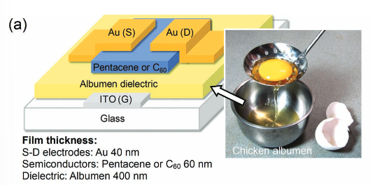
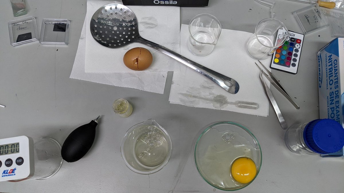
2/9 First thing is to explain that the idea of using albumen as dielectric has been used already in organic semiconductors (cool stuff 👇), but we wanted to use it with 2D materials and nobody had tried yet.

onlinelibrary.wiley.com/doi/epdf/10.10…
Image
Sep 20, 2022 13 tweets 7 min read
Our work "Combining Freestanding Ferroelectric Perovskite Oxides with Two-Dimensional Semiconductors for High Performance Transistors" is published online (#openaccess). I prepared a thread to briefly explain what we did 👇 pubs.acs.org/doi/10.1021/ac… In the last 12 years the sci-community has learn a lot about techniques and tools to handle freestanding atomically thin layers thanks to the isolation of 2D van der Waals materials: doi.org/10.1039/C7CS00…
Mar 29, 2020 13 tweets 4 min read
With the COVID-19 situation scalating so fast our lab @icmmcsic has been closed down for almost 3 weeks now. #StayHomeStaySafe

I've been thinking about interesting experiments that can be carried out at home with basically no measurement tools at all.👇Thread in! Sometime ago I wrote a little paper about a method to characterize the mechanical properties of micro-fibers (like carbon fibers):

[article]


[preprint] https://t.co/hj6V6IkHssiopscience.iop.org/article/10.108…
arxiv.org/ftp/arxiv/pape…