Continuing to play with the SSG5060X-V demo, testing the LFO. This is normally used as the source for analog modulation, but you can also output it directly via a front panel port which is handy.
Note that the SSG output level is in Vpp and the DMM only reads in Vrms.
Note that the SSG output level is in Vpp and the DMM only reads in Vrms.


The LFO can also be used to produce DC signals, so you get a free DC reference/bias voltage generator.
The levels seem dead on, this test is 500 μV low. And some of that might be tolerance of the 50Ω terminator I have across the DMM.
The levels seem dead on, this test is 500 μV low. And some of that might be tolerance of the 50Ω terminator I have across the DMM.


At 1.0V DC output, still looking very good. <1 mV off nominal.

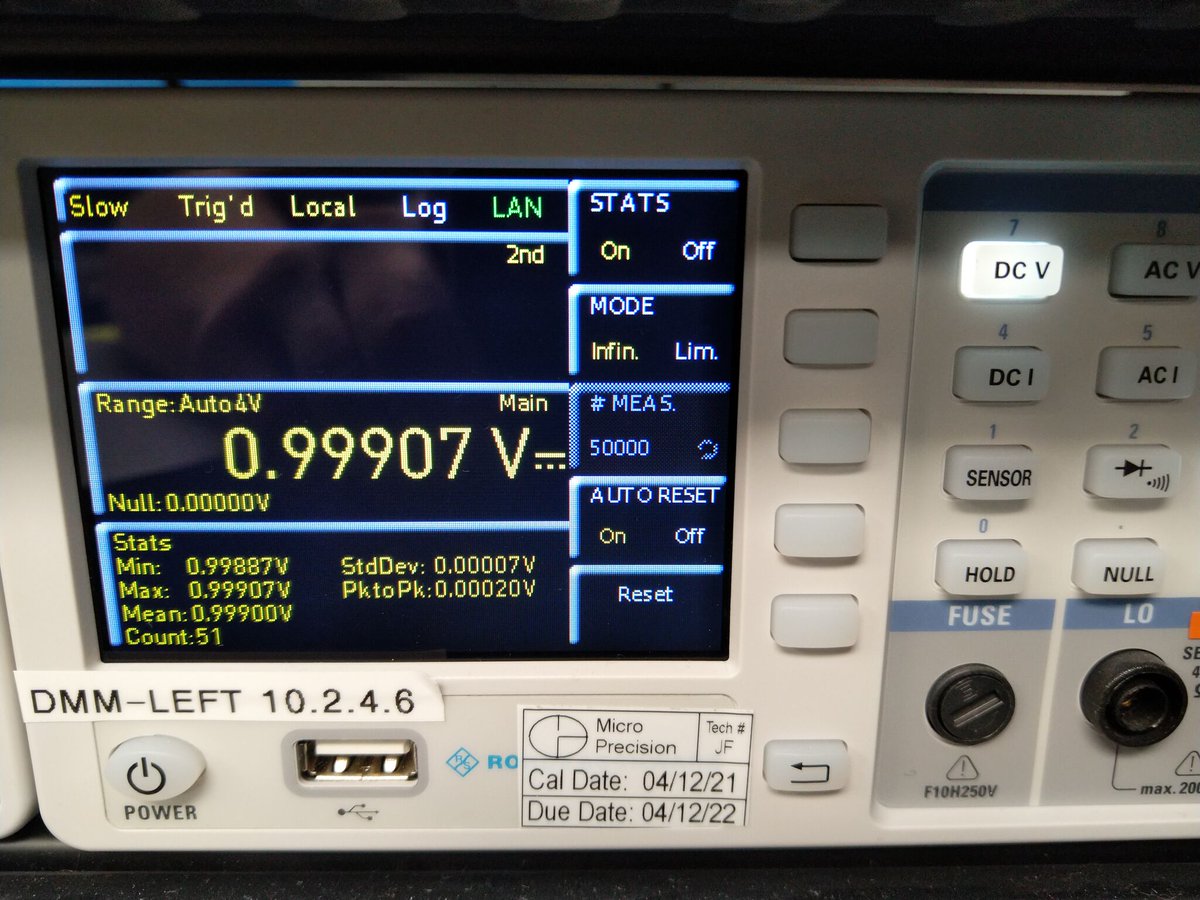
Frequency accuracy of the LFO is excellent as well. I suspect that my multimeter is actually the limiting actor in this measurement, not the SSG.


In case anybody is wondering why they make SMA-to-banana-jack adapters, this is a perfect example of why!
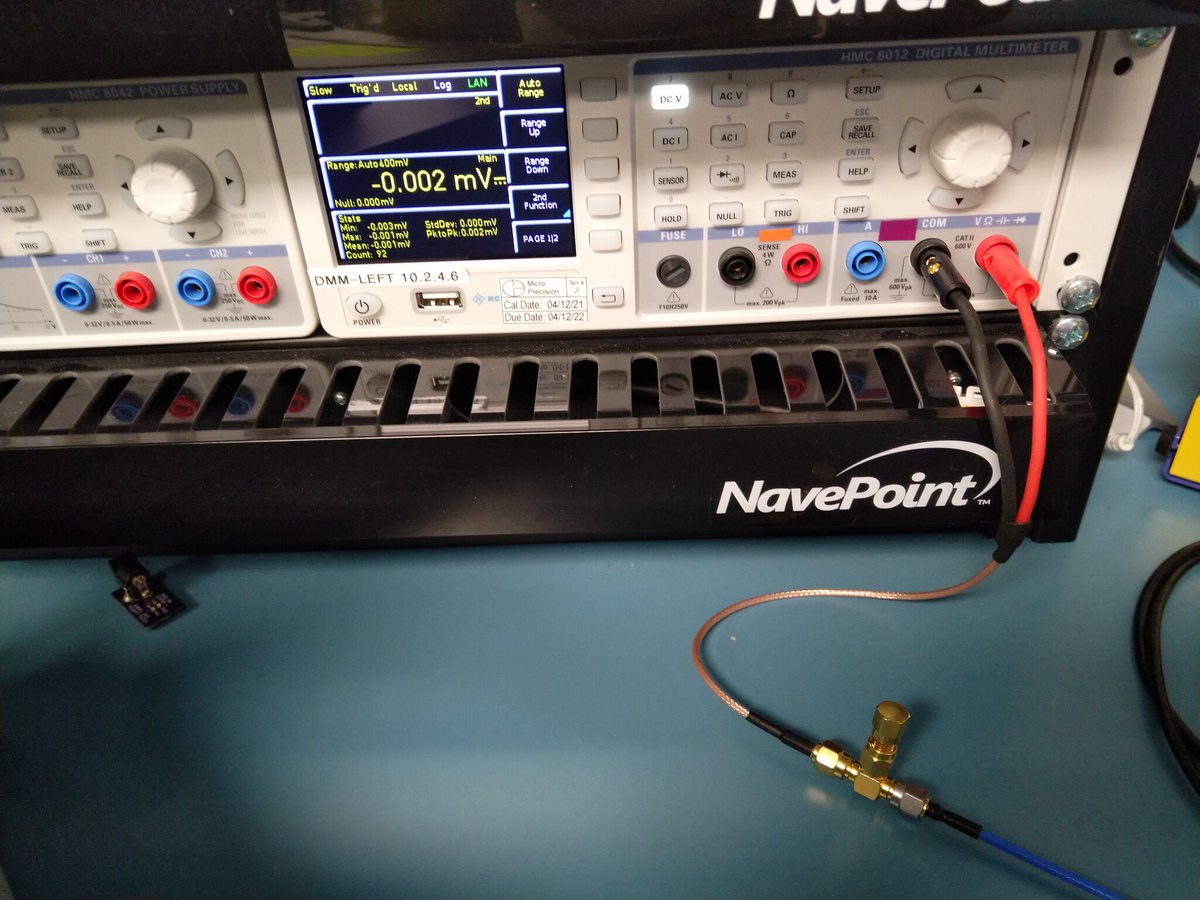
For the next test, I'm going to try to measure leakage between the RF and LF ports.
The LFO is outputting a 100 kHz sinewave at -40 dBm. I'm viewing it with my PicoScope 6824E to take advantage of the 12-bit ADC for improved sensitivity.
RF port is driving +10 dBm into 50Ω load
The LFO is outputting a 100 kHz sinewave at -40 dBm. I'm viewing it with my PicoScope 6824E to take advantage of the 12-bit ADC for improved sensitivity.
RF port is driving +10 dBm into 50Ω load

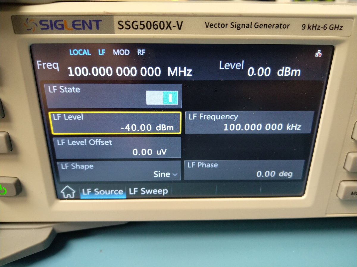
So we have a super weak LFO with an interferer 50 dB stronger in close proximity within the SSG.
Here's the LFO output spectrum with a 1 MHz +10 dBm RF signal on and off. Can you tell which is which? I can't. Excellent RF-LF isolation, any leakage is below the noise floor.
Here's the LFO output spectrum with a 1 MHz +10 dBm RF signal on and off. Can you tell which is which? I can't. Excellent RF-LF isolation, any leakage is below the noise floor.


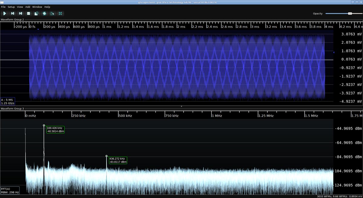
Maybe coupling is stronger at higher frequencies? Here's a 101 MHz test (there was a weak spur at 100 MHz present even with RF off - maybe leakage inside the PicoScope - that I wanted to avoid).
Again, no measurable leakage. Very happy.
Again, no measurable leakage. Very happy.


When I say "weak spur" I mean like -110 dBm.
It might actually be coming from the SSG but not the RF path? Seems to be present on the RF input (channel A) but weaker to absent on the floating input (F).
Not something I'm bothered by in the slightest, though.
It might actually be coming from the SSG but not the RF path? Seems to be present on the RF input (channel A) but weaker to absent on the floating input (F).
Not something I'm bothered by in the slightest, though.

• • •
Missing some Tweet in this thread? You can try to
force a refresh