A discussion and curiosity is resolved now.
Van Gogh, which is used by Valve's Steam Deck, has 4 UMCs.
I expected 4x 16-Bit (a memory channel under LPDDR5 is actually 16-Bit wide).
The official spec claimed 5.5 Gbps (dual-channel), which didn't made sense to me.
It got corrected
Van Gogh, which is used by Valve's Steam Deck, has 4 UMCs.
I expected 4x 16-Bit (a memory channel under LPDDR5 is actually 16-Bit wide).
The official spec claimed 5.5 Gbps (dual-channel), which didn't made sense to me.
It got corrected
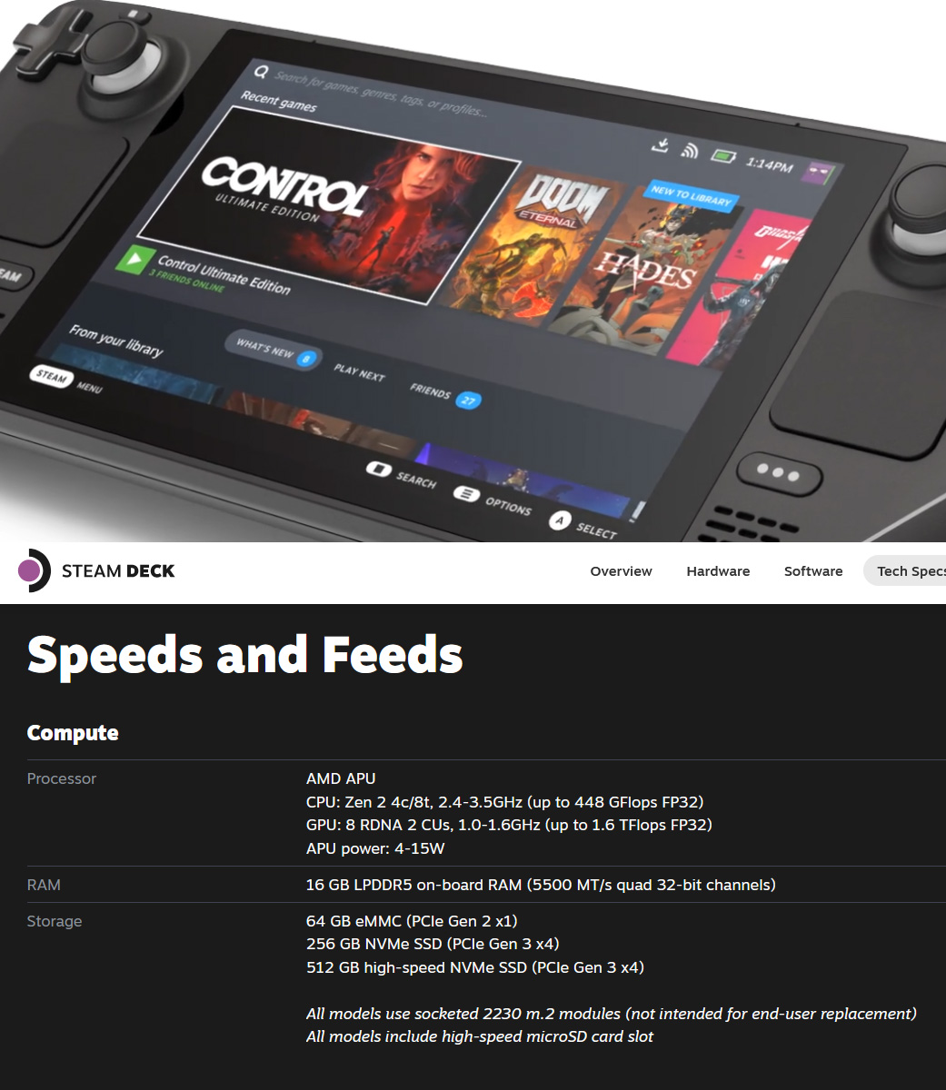
Valve claims now 4x 32-Bit (128-Bit) which fits to 4 UMCs.
It also means that as on Renoir/Cezanne, AMD is using a controller design with a 32-Bit granularity instead of 16-Bit channels.
Even 64-Bit LPDDR5 wouldn't have been bad for the Steam Deck specs but now bw looks great.
It also means that as on Renoir/Cezanne, AMD is using a controller design with a 32-Bit granularity instead of 16-Bit channels.
Even 64-Bit LPDDR5 wouldn't have been bad for the Steam Deck specs but now bw looks great.
In comparison to current gen consoles, only from the GPU perspective, you get more GB/s per TeraFLOP.
A small comparison:
XSX: 46.09 GB/s per GPU TFLOP
XSS: 55.91 GB/s per GPU TFLOP
PS5: 43.58 GB/s per GPU TFLOP
Steam Deck: 53.72-85.94 GB/s per GPU TF
A small comparison:
XSX: 46.09 GB/s per GPU TFLOP
XSS: 55.91 GB/s per GPU TFLOP
PS5: 43.58 GB/s per GPU TFLOP
Steam Deck: 53.72-85.94 GB/s per GPU TF
Extra comments for expectations are probably necessary.
The GB/s per GPU FLOP comparison obviously doesn't consider other clients sharing the memory bus, the amount of memory channels and banks per system, the power&memory bandwidth split, the software stack differences, etc.
The GB/s per GPU FLOP comparison obviously doesn't consider other clients sharing the memory bus, the amount of memory channels and banks per system, the power&memory bandwidth split, the software stack differences, etc.
While 1280x800 is about half the amount of pixels vs. 1920x1080 (Xbox Series S) and the GB/s per GPU TFLOP is greater than on stationary consoles, game workloads outside of resolution either don't scale down or to a far lesser degree.
Geometry, gameplay logic, audio systems, etc
Geometry, gameplay logic, audio systems, etc
The Steam Deck has less than half of the CPU power, the GPU also has strongly reduced fixed function geometry capabilities.
Low level APIs and optimizations, as on consoles, are not available.
Don't expect Xbox Series/PS5 experience, or even better, in 1280x800.
Low level APIs and optimizations, as on consoles, are not available.
Don't expect Xbox Series/PS5 experience, or even better, in 1280x800.
• • •
Missing some Tweet in this thread? You can try to
force a refresh