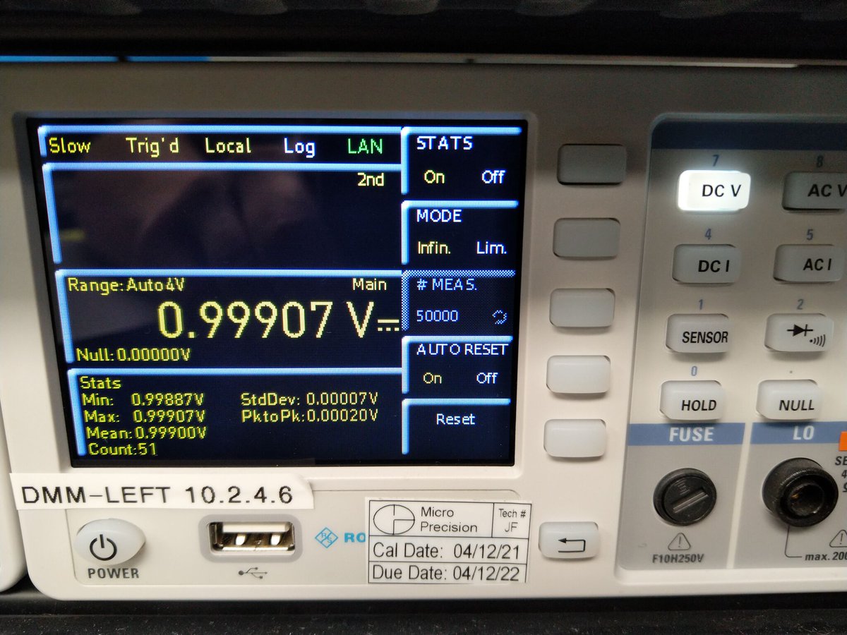
Finally finished initial characterization of the @UCSC_OpenRAM OR1 test chips made on SKY130! Here's a thread of results.
I tweeted a bunch of preliminary results a while back but some of the numbers have changed due to methodology tweaks and refining of the test protocols.
I tweeted a bunch of preliminary results a while back but some of the numbers have changed due to methodology tweaks and refining of the test protocols.
The OR1 test chip is an 8kbit (256 row x 32 bit) SRAM array with two bits of each byte bonded out to pins of a 64-pin QFN.
So the actual addressable capacity for the purposes of testing is 256 rows x 8 bits.
It predates full top level STA in OpenROAD and there are some very long routing delays at the top level. As a result, performance of the test chip is quite a bit worse than the "naked" SRAM IP.
It predates full top level STA in OpenROAD and there are some very long routing delays at the top level. As a result, performance of the test chip is quite a bit worse than the "naked" SRAM IP.
Additionally, performance is limited by the relatively slow I/O cells on the test chip.
However, it provides some good lower bounds on performance as well as allowing basic functionality verification, retention voltage tests, etc.
However, it provides some good lower bounds on performance as well as allowing basic functionality verification, retention voltage tests, etc.
The test platform used consists of two boards.
First, we have the "brain" (github.com/azonenberg/sky…).
First, we have the "brain" (github.com/azonenberg/sky…).


This board consists of a Xilinx Spartan-7 FPGA to run the hard real-time portion of the testing interacting with the SRAM, and a STM32F031 microcontroller which runs a text console allowing you to request specific tests, and does high level sequencing of FPGA operations.
Firmware for these devices is at github.com/azonenberg/sky….
The socket for the DUT is supplied with a fixed 3.3V rail for the I/O cells (also driving the FPGA I/Os and the STM32).
The socket for the DUT is supplied with a fixed 3.3V rail for the I/O cells (also driving the FPGA I/Os and the STM32).
A second power rail, nominally 1.8V, supplies the SRAM IP and on-die routing buffers. This is driven by a power opamp buffering the output of a 12-bit DAC, allowing the core power rail to be finely adjusted under software control.
Here's a test of Vcore step response.
Here's a test of Vcore step response.
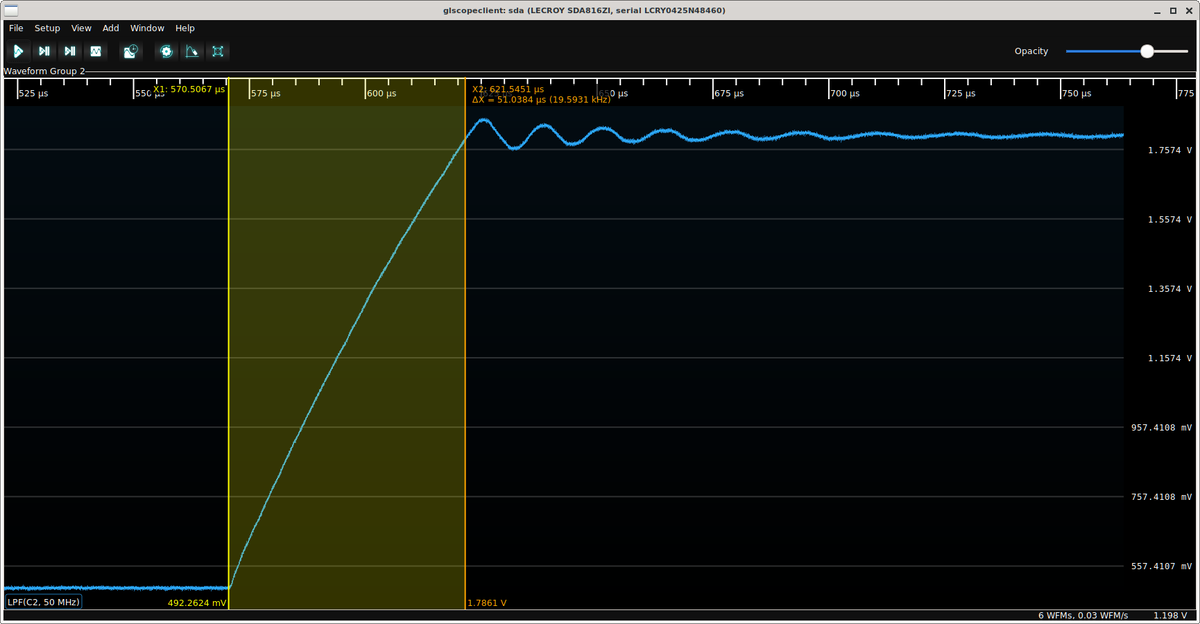
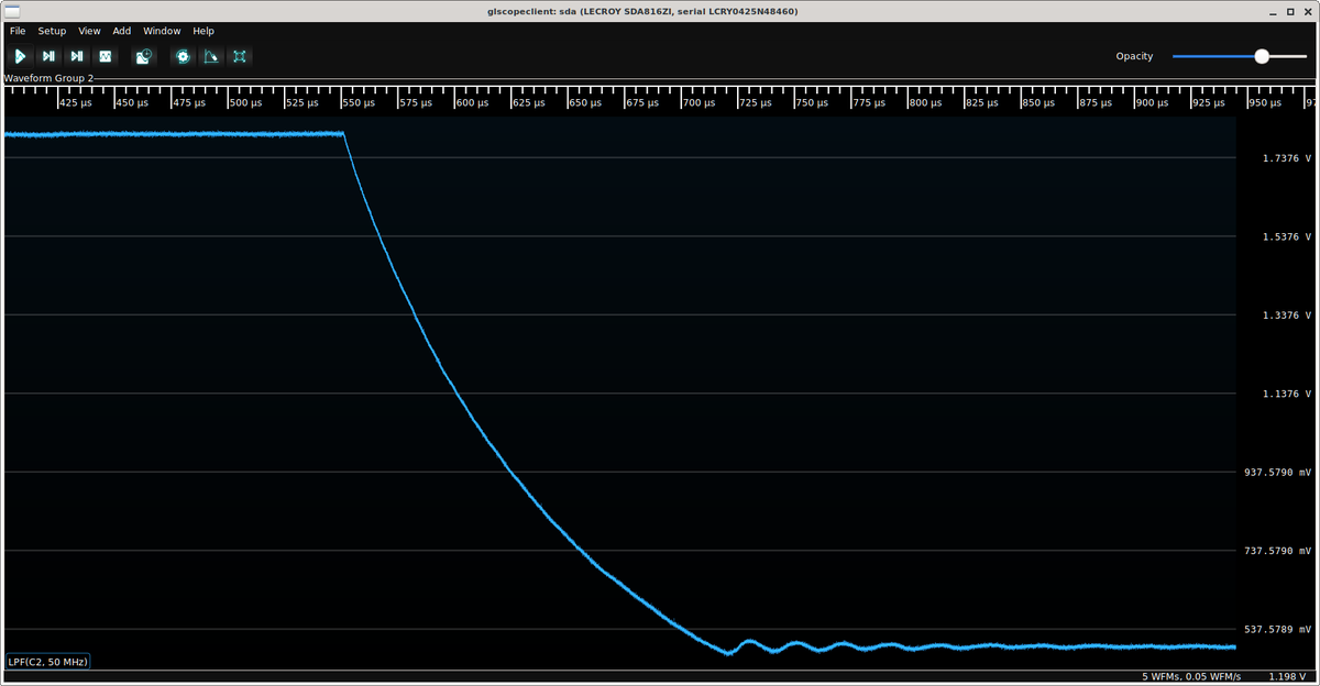
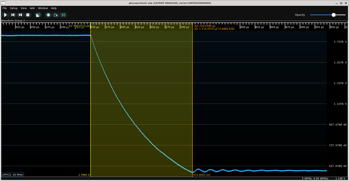
The second board, the "breakout", holds the actual OR1 test chip, test points for core and I/O power, and some bypass capacitors.
The combined path length on the breakout and host boards is tightly controlled to minimize skew interfering with performance measurements.
The combined path length on the breakout and host boards is tightly controlled to minimize skew interfering with performance measurements.
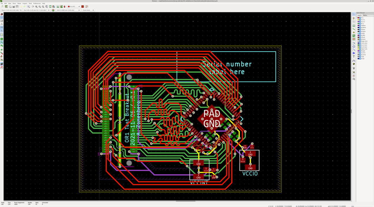
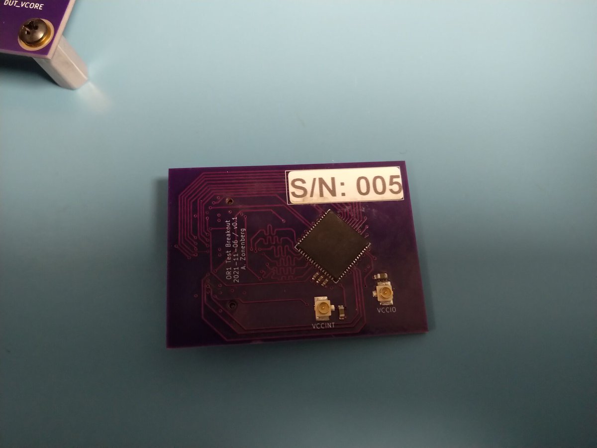
The test chip is placed against a Peltier plate (under an old x86 CPU cooler) to allow testing across thermal corners. A PT100 RTD mounted to the underside of the board allows me to see when we've hit thermal equilibrium and are ready to test.

Here's the three thermal corners I tested:
* Ambient: Peltier off, about 23C
* Heated: ~85C by FLIR on the top of the chip, and ~67C at back side by RTD
* Chilled: ~0C by FLIR on top of chip, and ~7C at back side by RTD.
* Ambient: Peltier off, about 23C
* Heated: ~85C by FLIR on the top of the chip, and ~67C at back side by RTD
* Chilled: ~0C by FLIR on top of chip, and ~7C at back side by RTD.
These are intended to roughly cover the 0 - 85C commercial temp range, but are not exact numbers.
The lack of a Peltier on the back of the board or a full environmental chamber means there's a thermal gradient, and exact Tj is unknown but probably between FLIR and RTD temps.
The lack of a Peltier on the back of the board or a full environmental chamber means there's a thermal gradient, and exact Tj is unknown but probably between FLIR and RTD temps.
Additionally, while the chip has good thermal contact (Arctic Silver 5 compound + weight of Peltier and heatsink) on the top side, the RTD is secured to the back of the PCB via Kapton tape and a rubbery thermal pad.
I forgot to remove soldermask on the breakout to provide a solid metal-to-metal thermal contact for the RTD as well. The RTD temp fluctuated a fair bit from test to test, so I primarily used it to determine when I had reached equilibrium rather than as a reliable TJ indicator.
Future test chips will be WLCSP packaged so much more intimate thermal contact between die and thermal plate. Additionally, I hope to include on die thermal sensing circuitry.
I think that's about it as far as the test setup and methodology. On to the results!
Again, these are lower bounds due to the poor top level routing and the slow I/O blocks.
Again, these are lower bounds due to the poor top level routing and the slow I/O blocks.
Most of these tests sweep one or two parameters for each of six test conditions: single and dual port operation at each of the three thermal corners.
The dual port tests access each bitcell simultaneously on ports 0 and 1 to ensure worst case read margin is tested.
The dual port tests access each bitcell simultaneously on ports 0 and 1 to ensure worst case read margin is tested.
In order to compensate for the on-die large routing delay in the test chip and the ~700ps of round trip PCB trace delay from FPGA to DUT and back, read data from the test chip is registered on the FPGA in I/O cell flipflops.
These FFs are clocked by a second phase of the FPGA PLL used for driving write data and command/address lines, with a software-controlled shift from the main clock domain.
Delayed capture allows us to capture the read data reliably despite the extremely long clock-to-out delay.
Delayed capture allows us to capture the read data reliably despite the extremely long clock-to-out delay.
These registers are then shifted into the main FPGA clock domain and compared against the expected readback data.
So the first test I ran was "fpshmoo" which sweeps operating frequency vs read capture delay to find the optimum capture timing for future tests.
So the first test I ran was "fpshmoo" which sweeps operating frequency vs read capture delay to find the optimum capture timing for future tests.
This test is done at 1.8V only. Here's results for dies 1 to 4. Numbers in each cell indicate how many of the six corners we saw failures in (0 meaning fully functional).
Larger delays improve performance up to a point (more setup time), until we start seeing hold time issues.
Larger delays improve performance up to a point (more setup time), until we start seeing hold time issues.
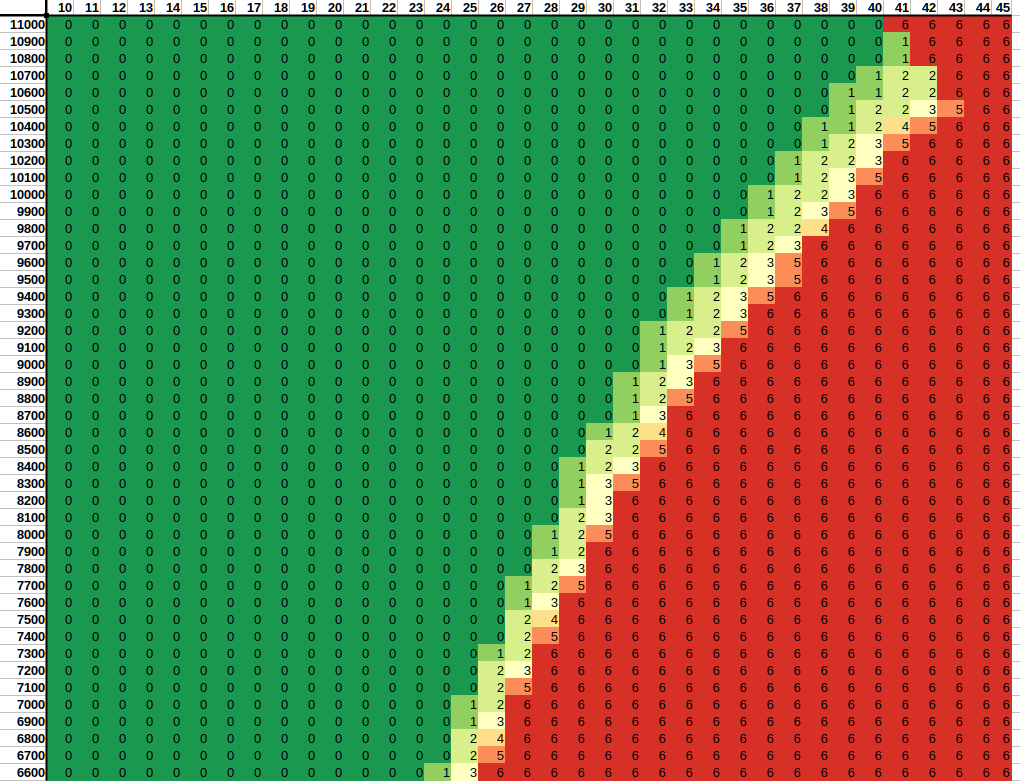
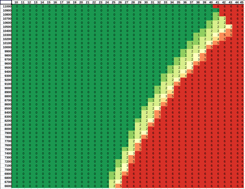
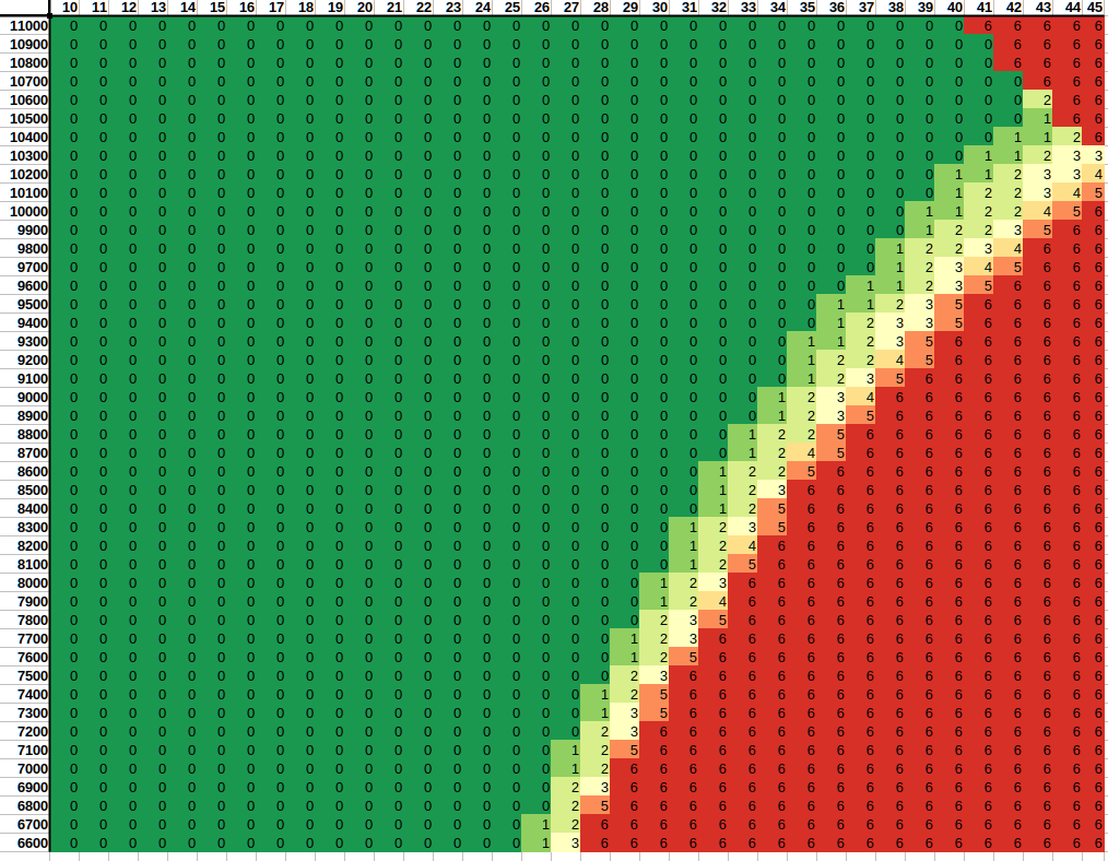
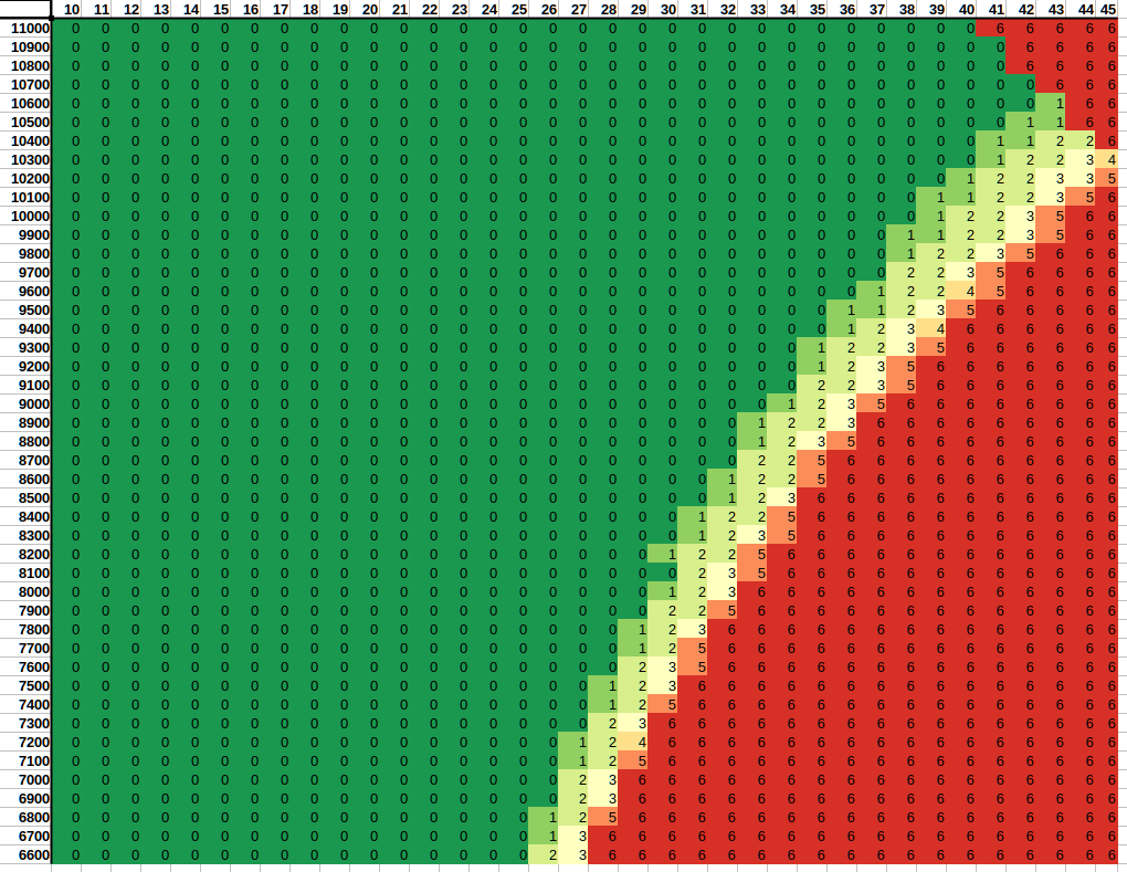
Optimal read capture delay for this test (read-then-write) is around 10.6 ns or 10600 ps, giving a Fmax of around 41-42 MHz.
I ran all of the remaining tests with 10.0 ns of read capture delay to provide extra hold time for the read-during-write scenario.
I ran all of the remaining tests with 10.0 ns of read capture delay to provide extra hold time for the read-during-write scenario.
Raw CSV data as well as the PHP shell scripts (sorry) that I use for preprocessing the data and the LibreOffice spreadsheets I use for rendering the shmoo plots can be found in the appropriate subdirectories here:
github.com/azonenberg/sky…
github.com/azonenberg/sky…
As of this writing all of the raw data has been pushed.
I'm postprocessing data as I tweet and pushing results as I go, so the spreadsheets and summary data for stuff I haven't tweeted about may lag behind the CSVs.
I'm postprocessing data as I tweet and pushing results as I go, so the spreadsheets and summary data for stuff I haven't tweeted about may lag behind the CSVs.
Anyway, that's dies 1 to 4, But what about die #5? The fpshmoo plot for that gives some very interesting results.
At exactly two test conditions, it doesn't work at certain frequencies.
At exactly two test conditions, it doesn't work at certain frequencies.

Inspecting the raw data CSV data I linked above, we can see these two conditions are single/dual port hot.
We see the expected massive numbers of errors in the bottom right (too fast/not enough capture delay) but also just a handful of errors seen at lower frequencies.
We see the expected massive numbers of errors in the bottom right (too fast/not enough capture delay) but also just a handful of errors seen at lower frequencies.
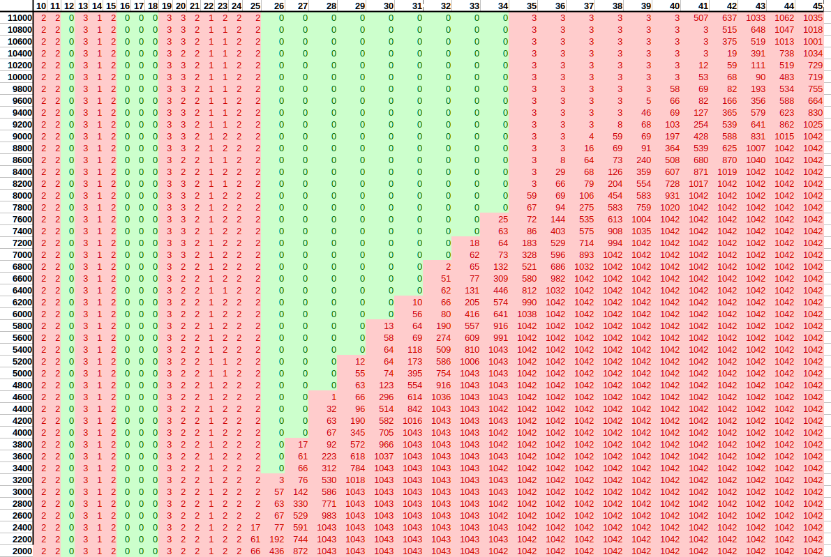
I'm not entirely sure why these failures seem to be timing sensitive, but it seems clear that die #5 has a handful of weak bit cells that start to malfunction when they get too hot but work fine at room temperature or when cold.
Picking up the thread after a snack...
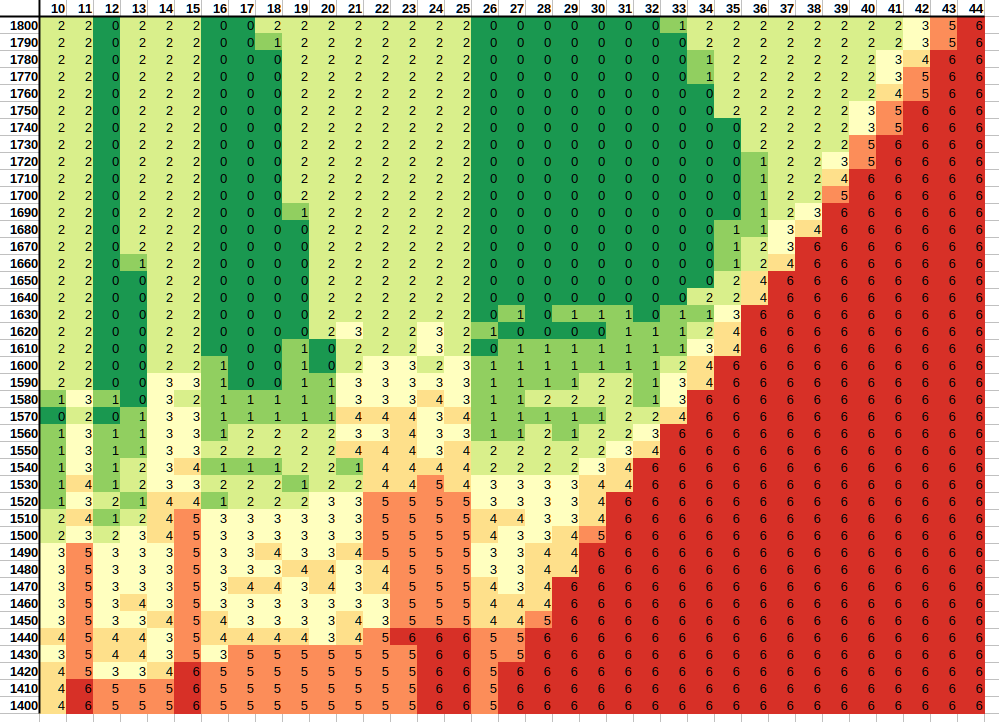
The next test is "fvshmoo". Same setup but plotting frequency against operating voltage with read capture delay held constant at 10 ns.
The next test is "fvshmoo". Same setup but plotting frequency against operating voltage with read capture delay held constant at 10 ns.
Die 1 is the best overall. 2 degrades rapidly at low voltage, but is still pretty fast if you don't let it dip. 3 is slower still and has a patchwork of degradation at low voltage, while 4 is only a little behind 1.
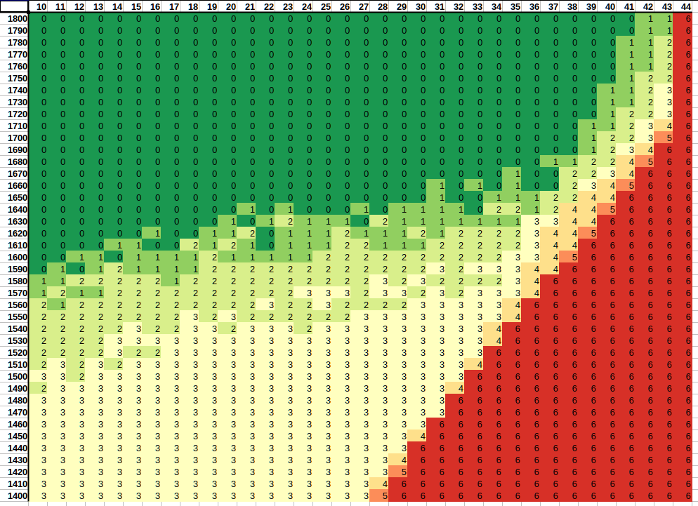
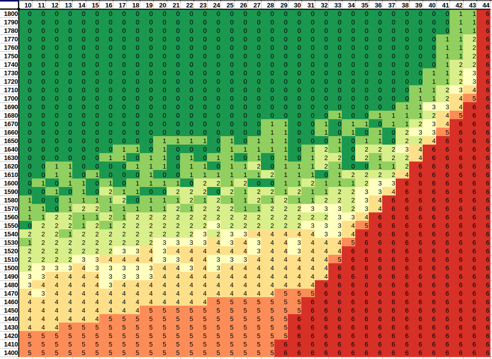

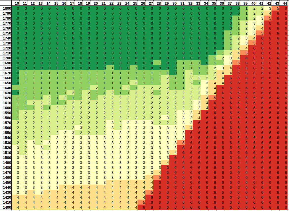
And then we get to die 5 with the weak cells. Unsurprisingly, low voltage makes them worse.
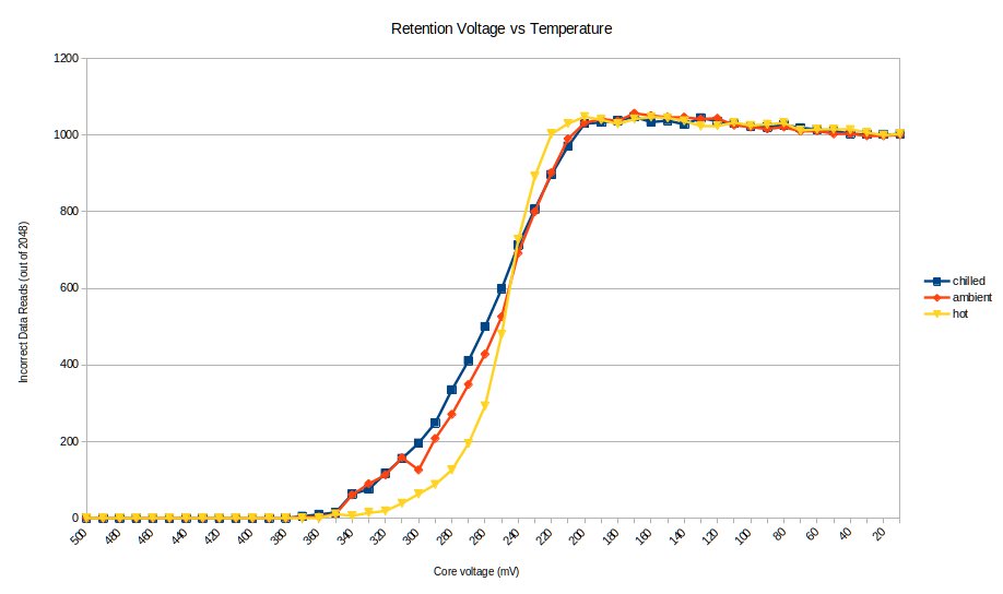
Next, we get to the retention test. This is intended to characterize the behavior of the memory in a deep sleep mode, where nothing is toggling and you're running a little bit of memory off a backup battery or something (with nothing reading or writing).
For this test we fill the memory with a test pattern at 1.8V, dip the voltage down to the test level for 10 seconds, bring back up to 1.8V, and read back.
All accesses are done at a sedate 12.5 MHz, since this is a test of static performance rather than dynamic behavior.
All accesses are done at a sedate 12.5 MHz, since this is a test of static performance rather than dynamic behavior.
All dies see worse retention behavior when cold; at high temperature you can drop ~30 mV further before you start losing data.
At ambient die 1 starts to fail at 420 mV, die 2 at 400, die 3 at 440, and die 4 at 440.
At ambient die 1 starts to fail at 420 mV, die 2 at 400, die 3 at 440, and die 4 at 440.


Die 5 is again quite interesting: it has the best low voltage performance of the lot at ambient/high temperatures (failing at 370/350 mV) but has a single bit error at 500 mV when cold.
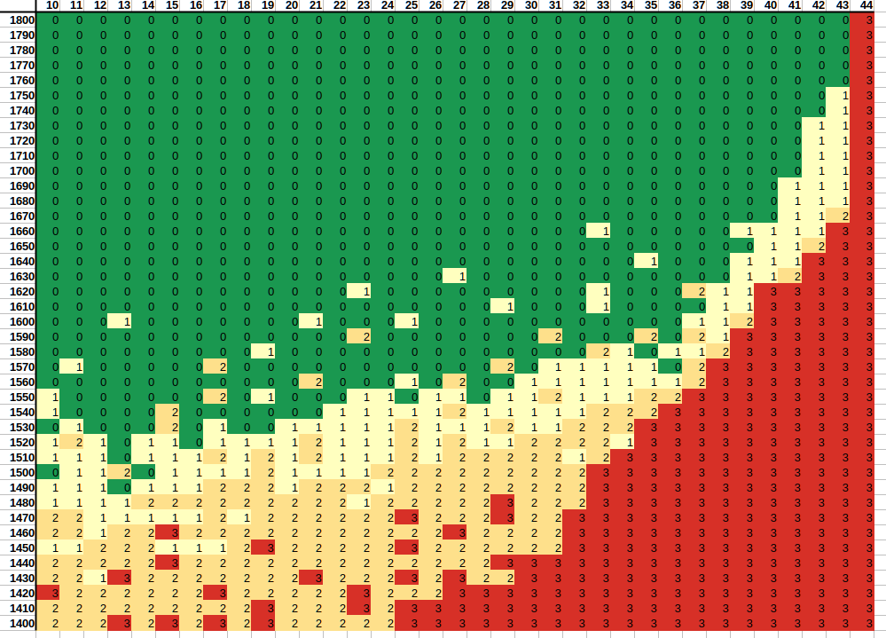
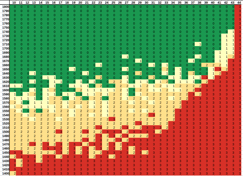
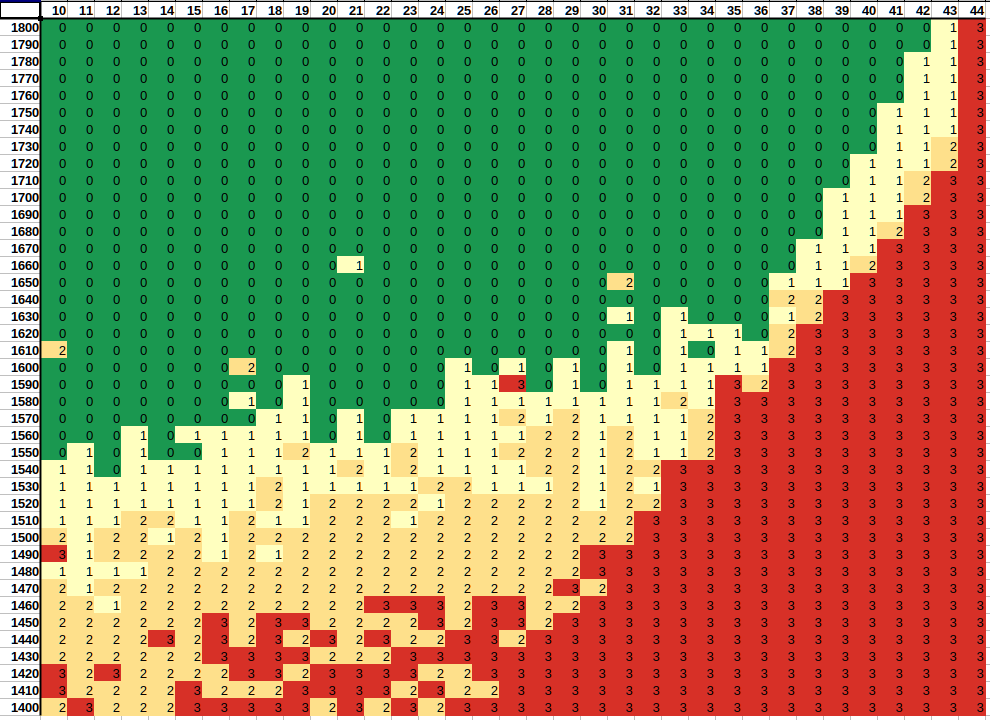
The next test is "rwshmoo". It's basically the same as "fvshmoo" but instead of filling the memory and reading back later, we do simultaneous readback during the write.
This can be more demanding on margin since the bitlines have to flip the bit cell *and* drive the sense amp.
This can be more demanding on margin since the bitlines have to flip the bit cell *and* drive the sense amp.
Here's rwshmoo results for die 1 to 4.

And finally, die 5. Note the absence of any vertical striping from the bad cells.
Numbers on these plots go from 0 to 3 because there's no single/dual port readback option available, rwshmoo is dual port by definition but one port is writing while the other reads.
Numbers on these plots go from 0 to 3 because there's no single/dual port readback option available, rwshmoo is dual port by definition but one port is writing while the other reads.
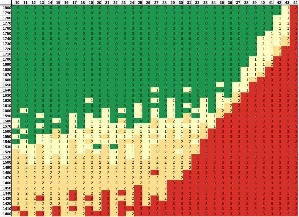
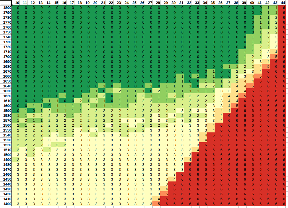
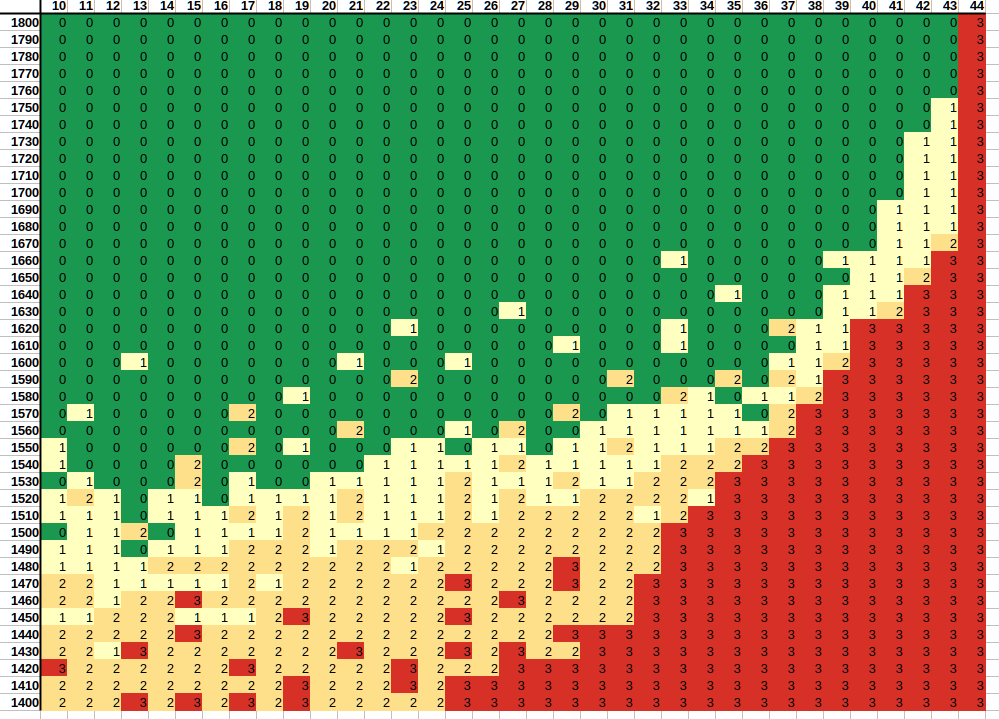
To my surprise, these results were substantially better than fvshmoo (write-then-read).
Maybe the extra drive current from the write circuitry in parallel with the bit cell provides more margin for reads?
Here's fvshmoo vs rwshmoo of die 1.
Maybe the extra drive current from the write circuitry in parallel with the bit cell provides more margin for reads?
Here's fvshmoo vs rwshmoo of die 1.
The final test is "vmap". This test runs at a constant 30 MHz and 10 ns read capture delay. and sweeps the voltage for the array to find the lowest voltage at which *each bit* will reliably store data.
The output is a 2D intensity-graded image with one pixel per SRAM cell.
The output is a 2D intensity-graded image with one pixel per SRAM cell.
The images are normalized so that the min/max operating voltage correspond top the min/max of the color ramp ("viridis" from matplotlib), meaning colors from one image to another are not directly comparable.
In general lighter colors mean the cell starts to fail at a higher voltage (weaker) while darker colors indicate a stronger cell.
Black cells had no observed failures across the entire 600 - 1800 mV sweep.
Black cells had no observed failures across the entire 600 - 1800 mV sweep.
This is generally the case for a handful of cells at the very bottom of the array, extremely close to the sense amplifiers so the voltage drop and R/C parasitics of the bit line matter less.
There's a total of 30 plots (5 dies * 3 temps * single/dual port) so I'm not going to tweet all of them, you can find them in or1/data/vmap/images/large/ in the repository.
But here's a few interesting ones.
But here's a few interesting ones.
Here's die 1 in dual port mode across all 3 temp corners (chilled, ambient, heated).
This die is pretty good. There's one weakish cell just below center that fails at 1530 mV when chilled. At ambient temp it fails at 1500 mV, and when hot it's good to 1450 mV.
This die is pretty good. There's one weakish cell just below center that fails at 1530 mV when chilled. At ambient temp it fails at 1500 mV, and when hot it's good to 1450 mV.



I forgot to mention, this is a stylized view of the actual die floorplan. There's two bytes per row with address 0/1 at bottom, then 2,3... up to fe/ff at the top.
Bits are numbered 0-7 L-R and interleaved so we have row0[0], row1[0], row0[1], row1[1]... row1[7].
Bits are numbered 0-7 L-R and interleaved so we have row0[0], row1[0], row0[1], row1[1]... row1[7].
Here's a less good die: die 5 at ambient temp. It looks like the column circuitry for bits 0, 2, 5, and 6 are all a bit weak, causing them to fail at higher voltage.

And here's a bar graph showing the average min voltage. Some of the bad columns fail over 100 mV before the good ones!
The fact that the failures are paired, rather than individual, rules out the physical bitline wires as the culprit.
The fact that the failures are paired, rather than individual, rules out the physical bitline wires as the culprit.
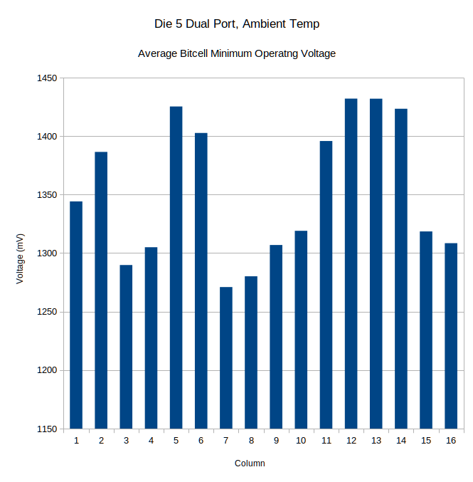
So whatever went wrong on this die is in the portion of the column read/write circuitry (or on die routing from SRAM to the I/O cells) that is common to both of the interleaved bits in the logical column.
And with that, I think that's all I've got! Feel free to ask questions or point out issues/errors in the methodology or results.
• • •
Missing some Tweet in this thread? You can try to
force a refresh