Time for a bit of a thread on all of my various open hardware oscilloscope probe projects, where they are, and what the next steps are on each project.
First off, the passive probes. All of these are resistive probes, so they have AKL-PT* part number prefixes (AntiKernel Labs, Passive, Transmission line).
The AKL-PT1 is a handheld probe that has bandwidth in excess of 6 GHz. Now that I've upgraded to an 8.5 GHz VNA I can characterize the true B/W limit, this data was from my old 6 GHz VNA.
It works well, but has a huge (+3 dB) peak in the response around 5 GHz.
It works well, but has a huge (+3 dB) peak in the response around 5 GHz.

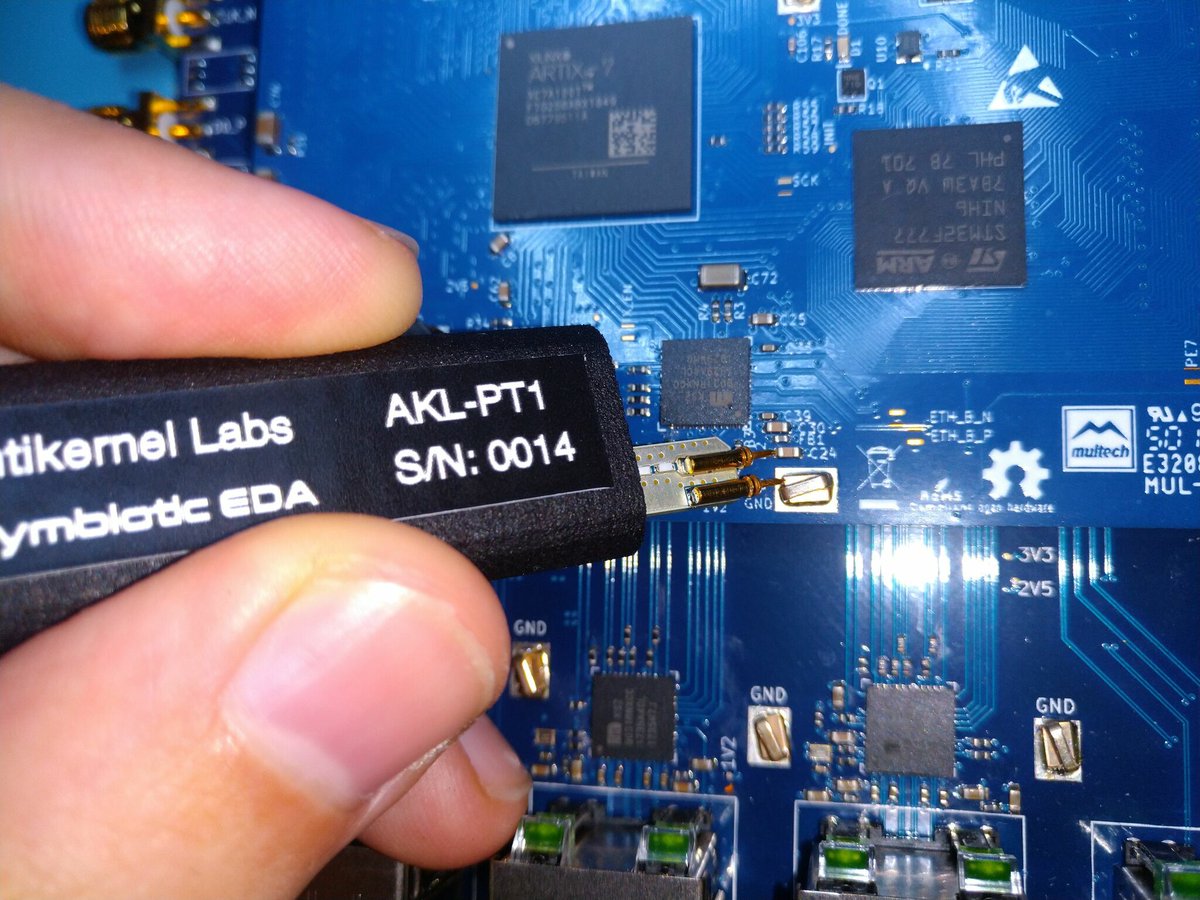
As far as I can tell, this peak is from reflections in the tip/socket assembly. I haven't touched it at all last year because I was focusing on solder-in probes, but would like to get back to it soon.
If anyone has ideas on how to flatten the response, let me know.
If anyone has ideas on how to flatten the response, let me know.
For now, it's reasonably usable out to at least 6 GHz but de-embedding is basically mandatory to get acceptable performance in broadband applications.
For narrowband work with a specan or for RF debug, you can just measure S21 in your band and apply a static gain correction.
For narrowband work with a specan or for RF debug, you can just measure S21 in your band and apply a static gain correction.
Next, the AKL-PT2. This is a 6 GHz solder-in probe built on flex PCB. Low BOM cost but fairly labor intensive to build due to the need to glue various stuff in place for stability, so not as cheap overall as I wanted.


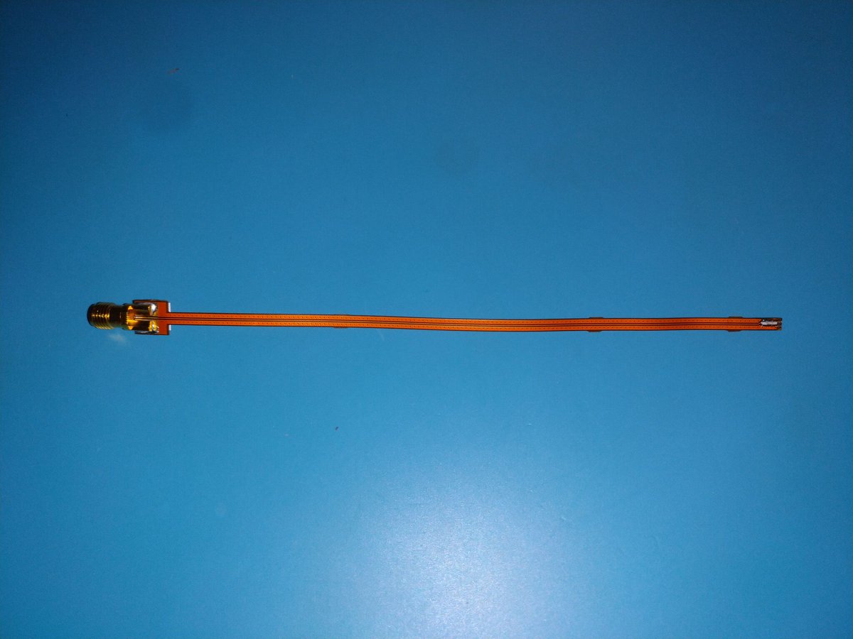
This one is done enough that I'm offering them for sale in low volume now, and have been for the past year or so.
They work decently, but have some limitations. Some can be fixed with a board spin, others are inherent to the architecture.
They work decently, but have some limitations. Some can be fixed with a board spin, others are inherent to the architecture.
They're a pain to solder. You can't reflow the SMA on the current rev because of the panel geometry, but that doesn't matter because the Amphenol 901-10511-3 connector tends to fall off the board in the oven because it's top heavy.

The connector also has to be be very carefully aligned, and there's no through-board pins to help with the process. Securing them during soldering requires a lot of Kapton tape and careful vise work.
So at some point I plan to respin w/ 901-10510-2 which has PTH alignment pins.
So at some point I plan to respin w/ 901-10510-2 which has PTH alignment pins.
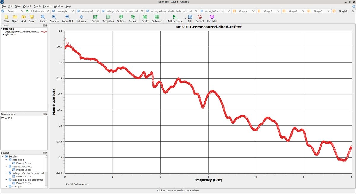
This spin will also slightly tweak the ground plane cutout under the SMA, which should help remove the ~0.5 dB p-p of ripple in the response of the current design.
The castellated tip soldered right to the test point provides extremely good input characteristics and high bandwidth. The main source of B/W limitation in the current rev is the long flex PCB "tail", which has fairly high loss.
Which leads to a straightforward path for improving bandwidth on these probes. Just make the tail shorter, and probably swap the SMA connector out with something else.
I'm leaning towards SMPM as it's a push-on connector that doesn't need torquing (difficult/risky on flex)
I'm leaning towards SMPM as it's a push-on connector that doesn't need torquing (difficult/risky on flex)
So I'm reasonably confident if I made a probe maybe 1/3 the length with a SMPM and the same/similar tip design that I could hit 10 GHz or more with quite flat response.
Probably going to try this some time in 2022, not sure on time frame yet.
Probably going to try this some time in 2022, not sure on time frame yet.
The same tip design that leads to such awesome bandwidth, however, is also the probe's greatest weakness.
With test points that aren't exactly 1mm left of a ground, you have to extend the ground lead which adds inductance.
With test points that aren't exactly 1mm left of a ground, you have to extend the ground lead which adds inductance.
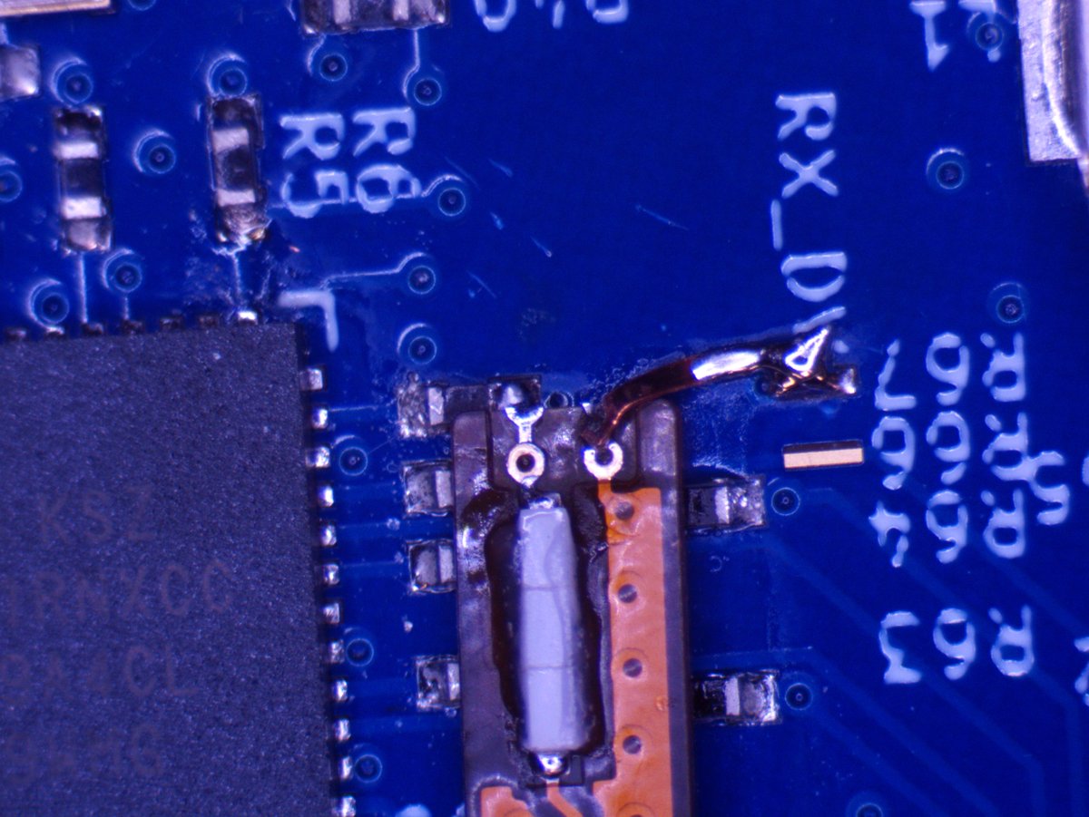
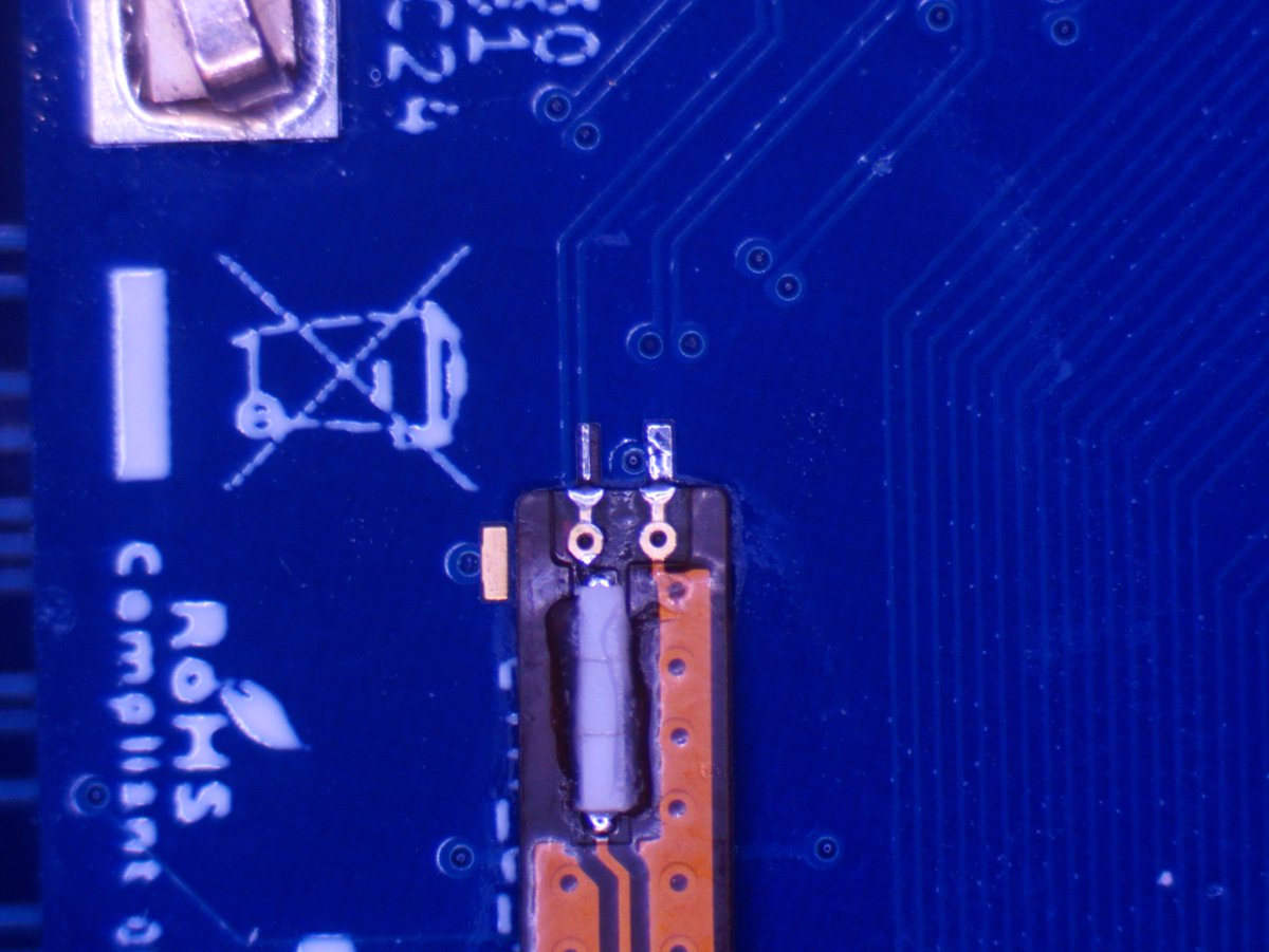
The castellated tip also has zero margin for flex/compliance. Any torque or shear loading applied to the probe will crack the solder joint, rip the castellation off the probe tip, or even potentially damage the DUT.
So firm mechanical support on the probe is absolutely critical.
So firm mechanical support on the probe is absolutely critical.
I plan to respin the PT2 with a new SMA some time in the indefinite near future to fix the ripples and assembly issues, but otherwise the design is final.
More comprehensive changes may happen, but will result in a new part number. It won't be an AKL-PT2 anymore.
More comprehensive changes may happen, but will result in a new part number. It won't be an AKL-PT2 anymore.
The AKL-PT3 is a ~2 GHz solder-in probe designed to be ultra low cost, basically disposable. It has the same tip as the AKL-PT2 but then jumps onto a U.FL rather than having a long tail.
Bandwidth was poor and it also had some mismatch at the connector launch.
Bandwidth was poor and it also had some mismatch at the connector launch.


This is, as far as I'm concerned, dead. It has all of the disadvantages of the AKL-PT2 but worse: equally fragile tip with no adjustable spacing, lower bandwidth, finicky U.FL connector with poor cycle lifetime, etc.
While I definitely could improve the flatness and bandwidth if I put the time into it, I just don't see the point. It doesn't do anything my other designs don't do better.
The AKL-PT4 - never seen publicly until now - is basically an AKL-PT1 repackaged in @SensePeek PCBite form factor. It needs a bit more work on the ground lead, but works beautifully to 3 GHz then starts peaking (I can probably add a filter to make it roll off instead).
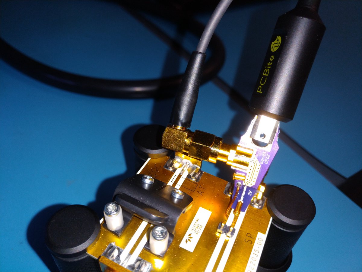
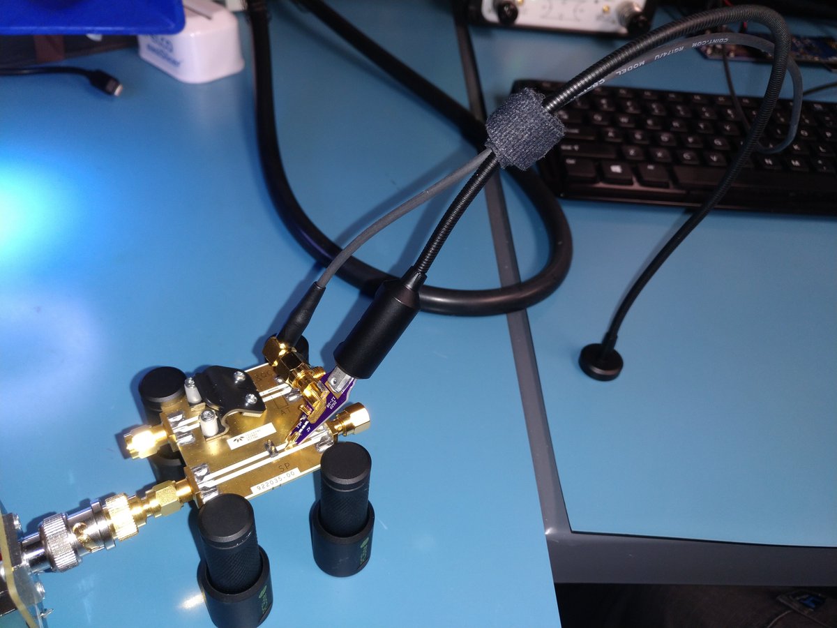
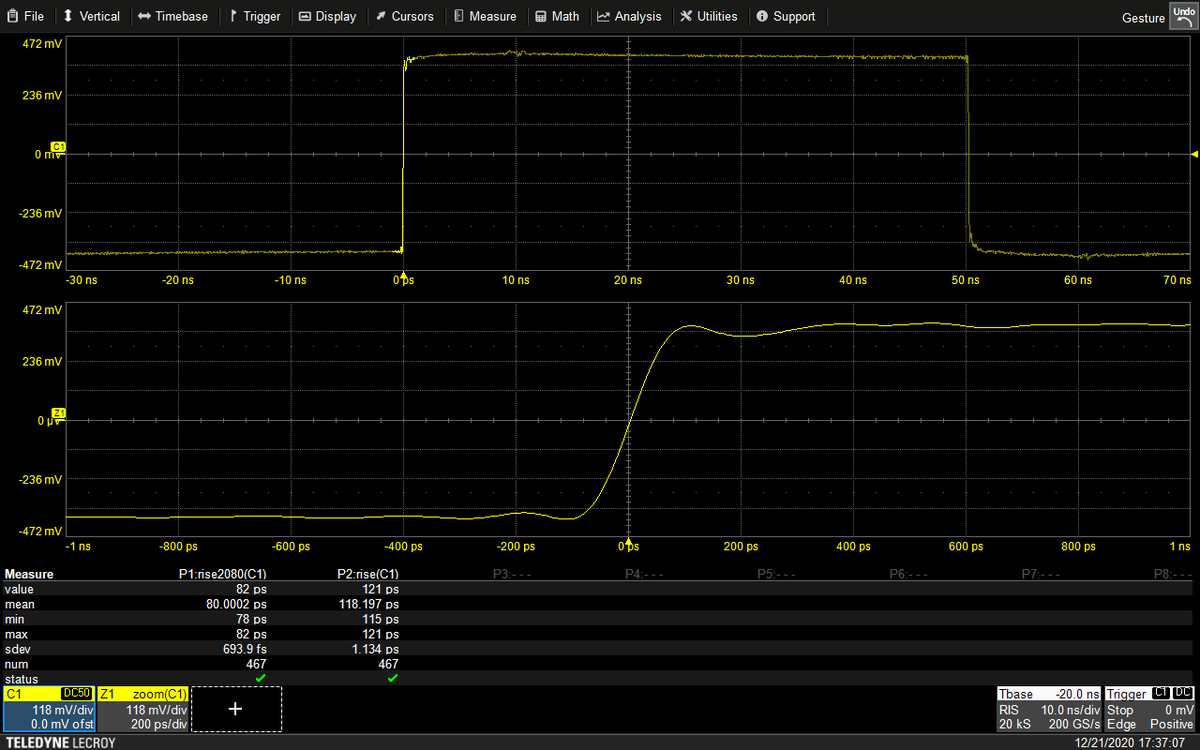

In late 2020 I had a very productive discussion with some engineers at SensePeek about a potential collaboration to develop such a probe, they sent me some positioner arms and the special mounting nuts (custom made, not available for sale), and indicated interest.
I sent some initial characterization data, including these plots, off to SensePeek shortly before Christmas 2020 and never heard back.
I never pursued the project further because without their support (to provide a source of the mount brackets) there was no point in continuing.
I never pursued the project further because without their support (to provide a source of the mount brackets) there was no point in continuing.
So it's been on ice all of last year. At some point in the indefinite near future I'd like to try to re-establish contact and figure out if they're still interested.
If not, I may try to pursue it on my own and get some custom CNC work done to make a compatible bracket.
If not, I may try to pursue it on my own and get some custom CNC work done to make a compatible bracket.
Finally, we get to my most recent passive probe design, the AKL-PT5.
This is a solder-in probe using Vishay HML01 axial lead tip resistors rather than castellations, allowing more flexibility of placement and tolerance to movement than the AKL-PT2.
This is a solder-in probe using Vishay HML01 axial lead tip resistors rather than castellations, allowing more flexibility of placement and tolerance to movement than the AKL-PT2.
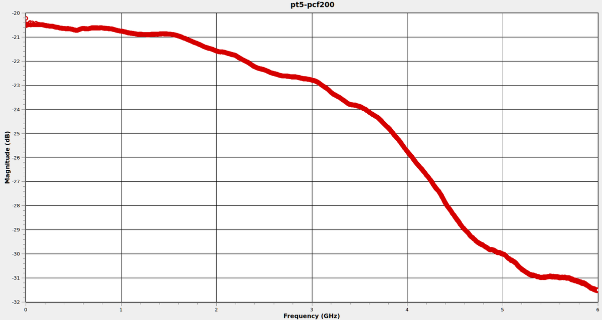
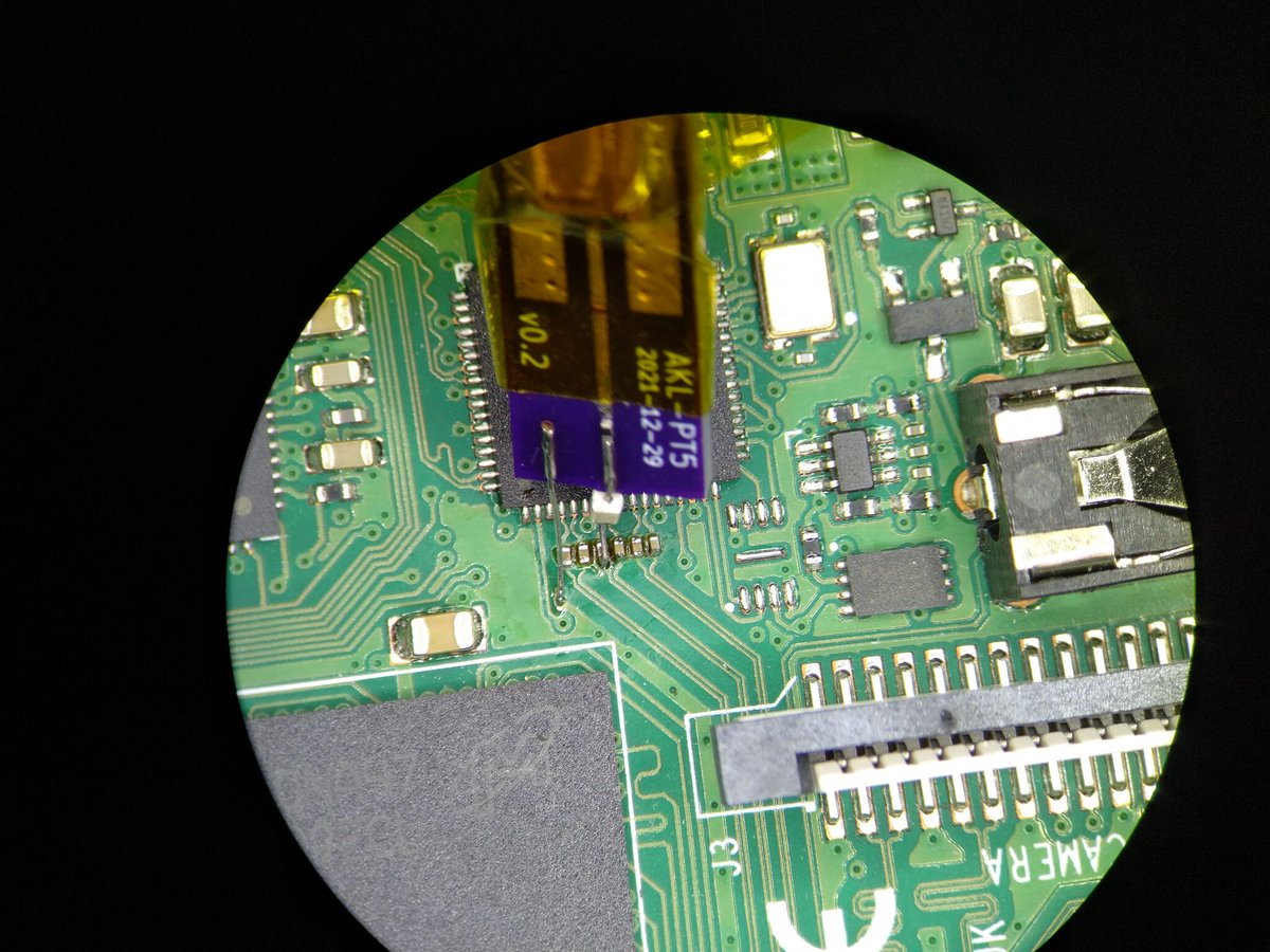
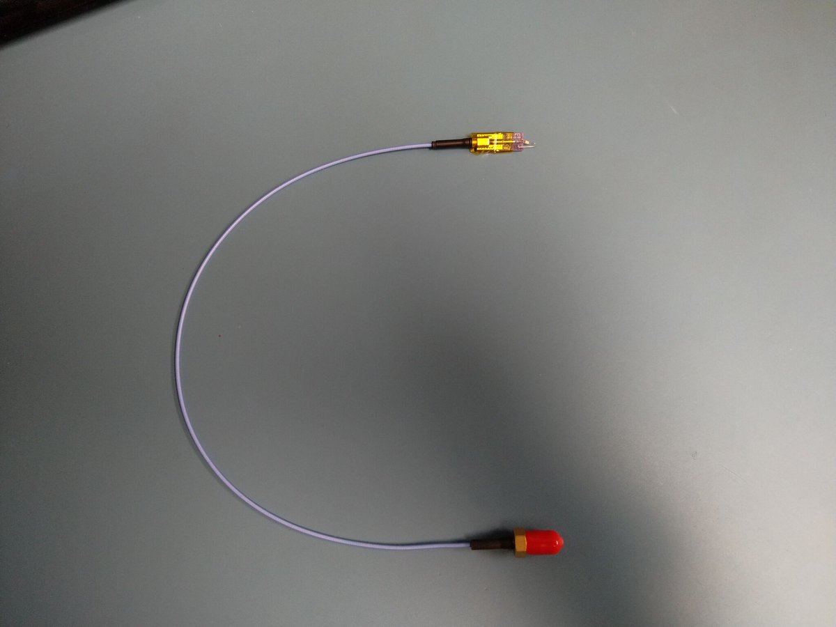

I have a second PCB rev at fab that should fix some minor issues, and want to try playing with different ratios of tip resistor to SMT resistor:
* 350 PCB + 100 tip (current)
* 200 PCB + 250 tip
* 0 PCB + 450 tip
I also want to try a HML01 0-ohm instead of wire as ground lead.
* 350 PCB + 100 tip (current)
* 200 PCB + 250 tip
* 0 PCB + 450 tip
I also want to try a HML01 0-ohm instead of wire as ground lead.
Testing the 250/450/0 ohm resistors, as well as going into higher volume production, will require navigating Vishay's custom order process because the HML01 is made-to-order part that they don't maintain inventory of or manufacture unless someone specifically asks.
This is my current R&D focus and as soon as I have the budget to do several custom resistor orders (they have a 100 piece minimum, so we're talking several kUSD investment for the three values plus higher volumes of the 100 ohm) I'll start trying the other values.
Next, we get to the active probes. All of my designs to date are differential (AKL-AD* part numbers).
First off is the AKL-AD1 amplifier (paired with the AKL-PD1 solder-in tip). This is a ~4 GHz active differential probe.
First off is the AKL-AD1 amplifier (paired with the AKL-PD1 solder-in tip). This is a ~4 GHz active differential probe.
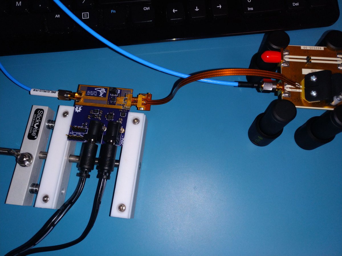

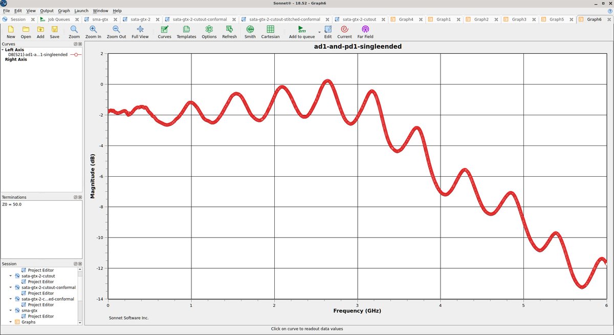
I was targeting something similar to what LeCroy does with their D4xx / D6xx WaveLink probes: a connectorized system with amplifier and tip mating via a duplex coaxial connector. This allows replacing or swapping tips, maybe a handheld browser tip, etc.
There's some mismatch somewhere on the path causing ripple in the response, but I could definitely correct for this with another few board spins and some better simulation.
The duplex SMPM connector is super expensive ($50ish for each side of the mated pair).
The duplex SMPM connector is super expensive ($50ish for each side of the mated pair).
It's good to 40ish GHz and total overkill for this project but I couldn't find any lower cost double-coaxial blind mate capable connectors. I might consider replacing it with a board to board rectangular connector like Samtec LSHM if I can get acceptable performance out of it.
The single biggest flaw in the current design is that the amplifier it uses (TI LMH6401) doesn't have great CMRR, making it more sensitive to common mode noise in the tip.
And the AKL-PD1 tip is a near perfect quarter wave dipole for the 2.4 GHz ISM band!
And the AKL-PD1 tip is a near perfect quarter wave dipole for the 2.4 GHz ISM band!
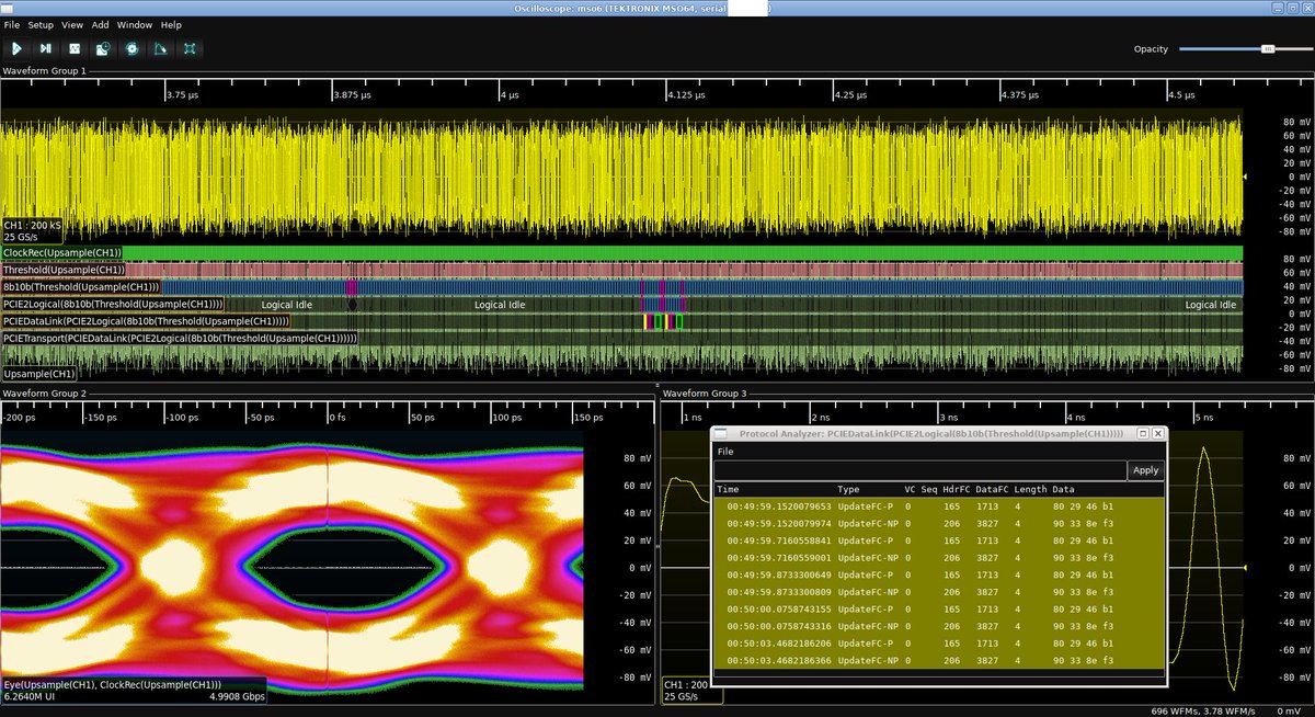
As long as you don't have any strong source of 2.4 GHz nearby (like, say, the wifi AP on the ceiling of my lab about 2m from the top of my bench that I test probes on...) it probably works great.
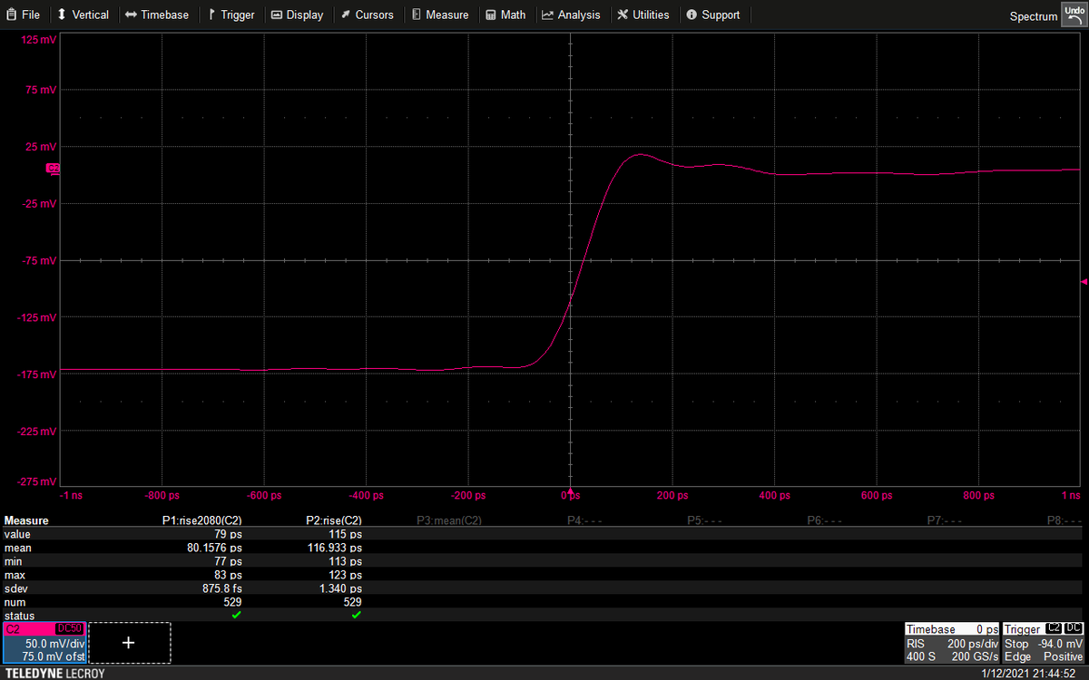
But the EMC issue ruins performance (note the eye closure from noise).
But the EMC issue ruins performance (note the eye closure from noise).
The AKL-AD1 is on ice for a little while but revisiting the general concept is a high priority.
I'll probably be switching to a different amplifier chipset, and replacing the castellated tips on the AKL-PD (basically two AKL-PT2s in parallel) with axial lead resistors a la PT5.
I'll probably be switching to a different amplifier chipset, and replacing the castellated tips on the AKL-PD (basically two AKL-PT2s in parallel) with axial lead resistors a la PT5.
The AKL-AD2 is a part number I reserved for a design I never made. It was to use the Analog Devices ADL5580, a 10 GHz fully differential amplifier with 100 ohm matched differential input. I actually have samples of them sitting around in my parts bin.
Its fatal flaw for use in a differential probe design is that while the input and outputs can be DC coupled, the input common mode ranges from 1.4 to 1.8V and the output common mode ranges from 400 to 700 mV.
I spent quite a while thinking about ideas for how to create a probe containing this amplifier that would give me DC coupled input and output, but have to date been unsuccessful.
One possible strategy still on the table is to make an AC coupled differential probe with it.
One possible strategy still on the table is to make an AC coupled differential probe with it.
This won't be usable for applications like DDR RAM signal integrity where DC voltage accuracy is critical and you don't have DC balanced data streams.
But for high speed serial work, it might actually work quite well. Multigigabit SERDES are often AC coupled anyway.
But for high speed serial work, it might actually work quite well. Multigigabit SERDES are often AC coupled anyway.
So maybe I'll make that one of my 2022 projects. I could pair it with a HML01 based AKL-PD1 variant and probably get very nice performance from a few MHz to high single digit GHz.
Finally, we get to the AKL-AD3: a differential browser probe. Response curve is beautiful and shows 6+ GHz of bandwidth... if you ignore the massive ripples and -12 dB dip at 1.57 GHz!


It seems like my problem here is a poor match at the input to the differential amplifier causing reflections in the flex PCB. I'm actively troubleshooting and need some more experiments to determine conclusively what I'm dealing with, and whether the connector is at fault too.
First step will be making some test fixtures that mate a pair of the connectors back to back so I can TDR/VNA them. That's on my list of things to do in the next few days.
Early results from measuring the amplifier board were inconclusive: the amplifier IC and connector were so close together on the PCB that I wasn't able to clearly separate the effects of one from the other.
I *think* there's a big dip in impedance at the connector, but not sure.
I *think* there's a big dip in impedance at the connector, but not sure.
• • •
Missing some Tweet in this thread? You can try to
force a refresh