Xilinx has a few app notes: xapp495 and xapp460.
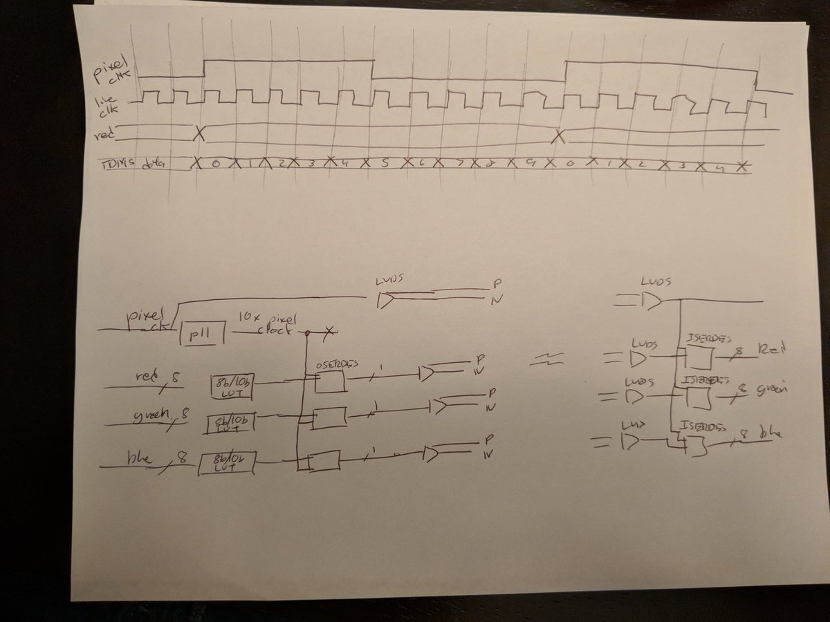
A few more words: tmds is 8b/10b encoded. That means for every 8 bit value there is a corresponding 10 bit value (a 1 to 1 look up table).
It uses LVDS (low voltage differential signaling) to transmit the data 1/n
So there are 8 wires, that represent 4 unique signals: Red, Green, Blue, Clock 2/n
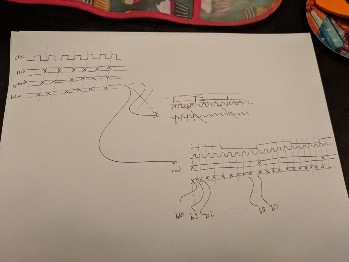
For every clock rising edge, we set the values on the "data bus" (red, green, blue).
We use a differential buffer to change the CMOS level to a LVDS level 3/n
For every clock edge, there is actually 10 bits of data. That's because we send the "raw" clock that represents the 10 bit value for each edge vs the "line clock" that represents 10x that speed.
4/n

RGB + clk into the OSERDES
RGB + clk out of the ISERDES.
6/n
Making sense?
Standing by for more questions!
7/7


